Electronic design automation (EDA) is the category of software tools engineers use to design, simulate, and verify electronic systems before a single PCB is fabricated. If you think EDA just means “schematic capture,” you are missing most of what modern EDA toolchains actually do. This article explains what electronic design automation tools do, how they differ from each other, and what to look for when selecting an EDA platform for PCB work.
What Electronic Design Automation Actually Covers

At minimum, an electronic design automation toolchain handles four stages:
- Schematic capture: Drawing the logical circuit. This is where you place symbols, wire connections, and assign component values. A good schematic tool also manages hierarchical sheets, design rule checks (DRC), and electrical rule checks (ERC).
- PCB layout: Translating the schematic into a physical board. The PCB editor places footprints, routes copper traces, defines plane layers, and applies design rules for clearance, impedance, and manufacturability.
- Simulation and analysis: SPICE simulation for analog circuits, signal integrity analysis for high-speed digital, thermal simulation, and power distribution network (PDN) analysis. These run inside or alongside the EDA tool.
- Manufacturing output: Generating Gerber files, drill files, pick-and-place data, and assembly drawings. Errors at this stage create fabrication rejects.
For more on schematic best practices, see ReversePCB’s PCB schematic design guide.
Major EDA Platforms for PCB Design
The EDA landscape splits roughly into three tiers, and picking the wrong one for your project causes real pain:
| Tier | Tools | Best For | Limitations |
|---|---|---|---|
| Open-source / free | KiCad, EasyEDA, LibrePCB | Hobbyist projects, open hardware, 2-6 layer boards | Limited advanced simulation, less robust library management |
| Mid-range professional | Altium Designer, OrCAD, PADS | Professional 4-16 layer boards, high-speed design, team workflows | Subscription cost, steep learning curve |
| Enterprise / RF-specialized | Cadence Allegro, Mentor Xpedition, ADS | Complex multilayer, RF/microwave, HDI, rigid-flex | Very high cost, requires dedicated CAD support staff |
KiCad has closed the gap with mid-range tools for many designs. It is now a viable professional choice for boards up to about 8 layers, provided your team is comfortable with its library workflow. If you are designing a high-speed digital board with DDR memory or differential pairs at multiple GHz, Altium or Cadence-level signal integrity tools become harder to replace.
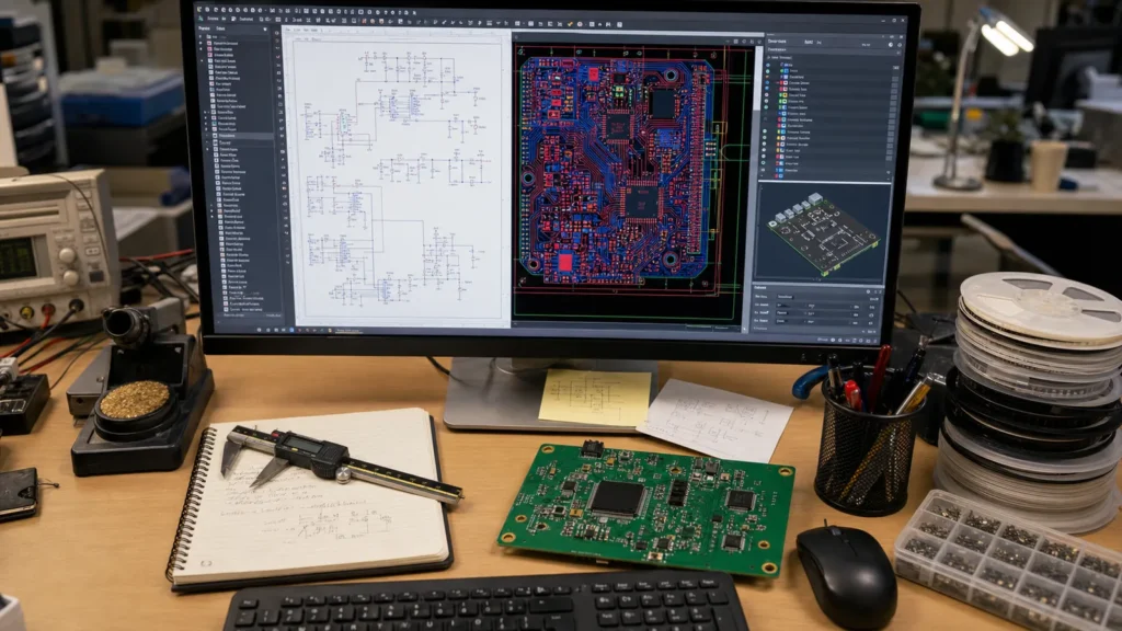
The Schematic-to-PCB Workflow in Practice
Here is what the EDA workflow looks like for a typical PCB project:
- Create the schematic. Place symbols, wire nets, assign footprints, and run ERC to catch unconnected pins or conflicting outputs.
- Generate the netlist. The netlist is a machine-readable list of every component and connection. The PCB layout tool imports it.
- Place components. Position footprints on the board outline. Group related parts, orient connectors correctly, and leave room for mounting holes and keep-out zones.
- Route traces. Connect pads according to the netlist, respecting clearance rules, trace width requirements, and impedance targets. Modern EDA tools include auto-routing, but critical nets should always be hand-routed.
- Run DRC. The design rule checker verifies that no trace violates clearance, no pad is missing a connection, and every net is fully routed. Passing DRC is the minimum requirement before sending a board to fabrication.
- Generate manufacturing files. Export Gerbers, NC drill files, BOM, and assembly drawings. Double-check the Gerber viewer — errors at this stage are expensive.
If you are moving from schematic to PCB in Altium specifically, this step-by-step guide walks through the full process.
What to Look For When Choosing an EDA Tool
Focus on what actually affects your project, not feature-count marketing:
- Library quality and management: Does the tool ship with verified footprints for the components you actually use, or will you spend hours creating symbols from datasheets? A weak library wastes more time than any missing simulation feature.
- Design rule capabilities: Can you define rules by net class, differential pair, and region? If you need controlled impedance, does the tool calculate trace geometry from your stackup?
- Collaboration: Can multiple engineers work on the same project? Does it support version control? Git integration is increasingly standard in modern EDA tools.
- Manufacturing output reliability: Do the Gerber exports match the board as-designed? Some tools silently apply design rule corrections during output that change the board. Verify in a Gerber viewer every time.
- Simulation integration: If you rely on SPICE simulation, does the tool integrate it natively, or do you need to export netlists to an external simulator?
Common EDA Mistakes That Reach Fabrication
- Unrouted nets passing DRC: Some tools allow unrouted nets to pass DRC if they are marked as “no-connect.” Verify every net visually or with a connectivity report.
- Footprint pin 1 mismatch: The schematic symbol and PCB footprint disagree on pin 1 orientation. This is the most common cause of first-revision board failures. Always visually verify pin 1 indicators on every IC footprint.
- Silkscreen overlapping pads: Silkscreen printed on copper pads prevents soldering. Most tools have a silkscreen-to-pad clearance rule — enable it.
- Unmatched impedance: The trace geometry in the layout does not produce the target impedance because the stackup was defined incorrectly in the tool. Verify impedance with the fabricator’s actual stackup, not the tool’s default.
Frequently Asked Questions
What is electronic design automation?
Electronic design automation (EDA) is a category of software used to design electronic systems, including schematic capture, PCB layout, circuit simulation, and manufacturing file generation. EDA tools are essential for modern PCB development.
Is KiCad good enough for professional PCB design?
Yes, KiCad is now capable of professional-grade PCB design for boards up to about 8 layers. It supports differential pair routing, length tuning, and 3D visualization. For very high-speed designs requiring advanced signal integrity simulation, Altium or Cadence tools provide deeper analysis.
What is the difference between schematic capture and PCB layout?
Schematic capture is the logical design phase where you define component connections and circuit function. PCB layout is the physical design phase where you place components, route copper traces, and prepare the board for manufacturing.
Do I need simulation in my EDA tool?
For simple digital boards, simulation is optional. For analog circuits, power supplies, or high-speed digital designs, SPICE simulation and signal integrity analysis catch problems before fabrication and save revision spins.
What files does an EDA tool generate for manufacturing?
Standard manufacturing outputs include Gerber files (RS-274X or X2 format) for each copper layer, solder mask, and silkscreen; NC drill files; pick-and-place (centroid) files for automated assembly; and a bill of materials (BOM).