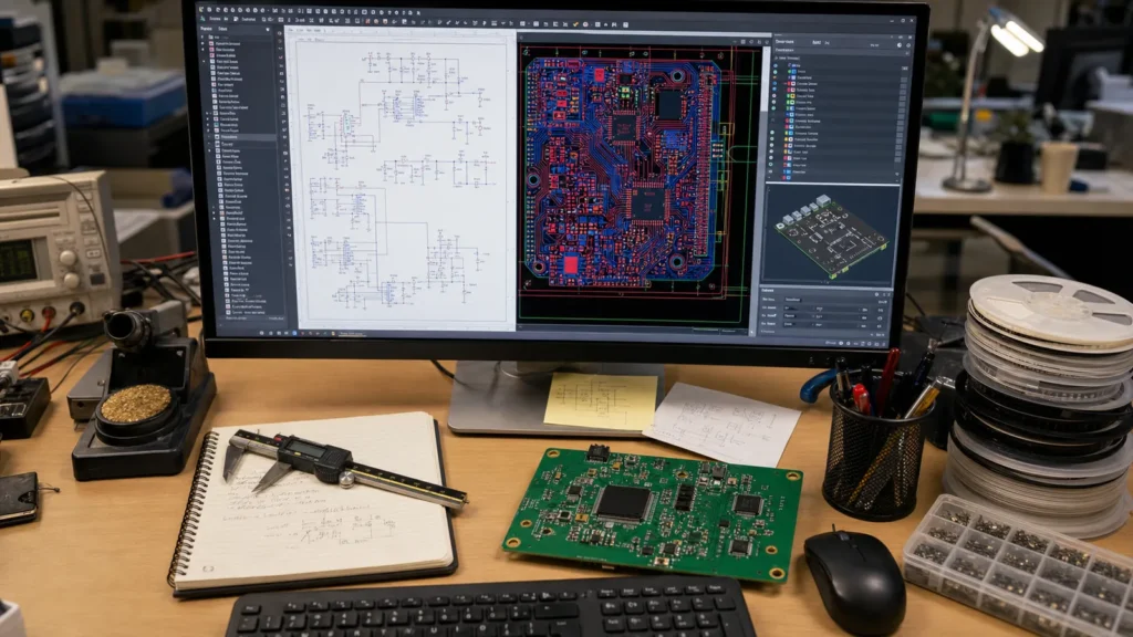
Automazione della progettazione elettronica (EDA) è una categoria che gli ingegneri del software utilizzano per progettare, simulare e verificare i sistemi elettronici prima della creazione di un singolo PCB. AspettoSe pensi che “She Schematics”, perderai la maggior parte di ciò che fa effettivamente la moderna catena di strumenti EDA. Questo articolo spiega come gli strumenti di automazione della progettazione elettronica siano diversi l’uno dall’altro e a cosa dovrebbero prestare attenzione quando si sceglie una piattaforma EDA per gli studi sui PCB.
Che cos’è in realtà l’automazione della progettazione elettronica?
almeno uno Automazione della progettazione elettronica La catena di strumenti elabora quattro fasi:
schema: Disegna un circuito logico. Qui è dove si impostano i simboli, i collegamenti dei cavi e i valori dei componenti. I buoni strumenti schematici riescono anche a controllare le pagine gerarchiche, le regole di progettazione (DRC) e le regole elettriche (ERC).
Layout PCB: Converti lo schema nella scheda fisica. L’editor di PCB inserisce impronte, tracce di rame, identifica i livelli dell’area e applica le regole di progettazione per le autorizzazioni, l’impedenza e le capacità di produzione.
Simulazione e analisi: Simulazione SPICE per circuito analogico, analisi dell’integrità del segnale per analisi digitale ad alta velocità, simulazione termica e rete di distribuzione di potenza (PDN). Funziona all’interno o accanto allo strumento EDA.
Potere di produzione: file Gerber, file di perforazione, dati di raccolta e posizionamento e immagini di montaggio. Gli errori in questa fase assicurano che la produzione venga rifiutata.
Per ulteriori informazioni sulle migliori pratiche schematiche, vedere. MANUALE REVERSEPCBs Disegno schematico.
La principale piattaforma EDA per la progettazione di PCB
Il paesaggio EDA è approssimativamente diviso in tre livelli e scegliere quello sbagliato per il tuo progetto provoca un vero dolore:
| Livello | Veicolo | il migliore | Limitazione |
|---|---|---|---|
| Risorsa aperta/gratuita | Kicad, Easeyeda, LibePCB | Hobby Project, Hardware aperto, Scheda a 2-6 strati | Simulazione avanzata limitata, gestione della libreria meno potente |
| Professionisti della classe media | Altium Designer, Orcad, Pad | Scheda professionale a 4-16 strati, design ad alta velocità, flusso di lavoro degli utensili | Tassa di abbonamento, curva di apprendimento ripida |
| Specializzazione aziendale/RF | Cadenza Allegro, mentore Xpedition, AD | Complesso multistrato, RF/Microdale, HDI, Rigido-Flex | Costo molto alto, personale di supporto CAD speciale |
KICAD ha colmato il divario con un veicolo a medio raggio per molti progetti. Ora è una scelta professionale adatta per schede fino a circa 8 strati, a condizione che il tuo team sia a suo agio nel flusso di lavoro della libreria. Alcuni GHzSe si sta progettando una scheda digitale ad alta velocità con memoria DDR o corrispondenza differenziale, lo strumento Altium Integrity Tool o il ritmo delle variazioni del livello diventa più difficile.
Flusso di lavoro schematico-PCB nell’app
Ecco la vista del flusso di lavoro EDA per un normale progetto PCB:
Crea schema. Posiziona i simboli per catturare i pin disconnessi o le uscite sovrapposte, la rete metallica, le impronte impostate e l’ERCEseguilo.
Crea netlist. Netlist è un elenco leggibile dalla macchina di ogni componente e collegamento. Lo strumento di layout PCB lo importa.
Posizionare i componenti. Posiziona le impronte sul contorno della tavola. Raggruppare le parti pertinenti, contrassegnare correttamente i connettori e lasciare spazio ai fori e alle zone di stoccaggio.
sentiero. netlist dei cuscinettiConnetti secondo e, segui le regole di autorizzazione, i requisiti di larghezza di traccia e gli obiettivi di impedenza. I moderni strumenti EDA includono il reindirizzamento automatico, ma le reti critiche dovrebbero essere sempre guidate manualmente.
RDCCorri bene. Il controller delle regole di progettazione verifica che non ci siano tracce che violano le autorizzazioni, che non ci siano collegamenti mancanti e che ogni rete sia completamente reindirizzata. RDCIl passaggio del consiglio è il requisito minimo prima di inviare il consiglio alla produzione.
Crea file di produzione. Esporta file di trapano gerber, NC, bombe e disegni di assemblaggio. Controlla di nuovo il visualizzatore Gerber – l’errore in questa fase è costoso.
Soprattutto l’AltiumPCB da schematicoSe passi a MANUALE Questo passo dopo passo attraversando un processo completo.
Cosa dovrebbe essere considerato quando si sceglie EDA Tools?
Concentrati su ciò che influisce effettivamente sul tuo progetto, non sul numero di funzionalità:
Qualità e gestione della biblioteca: Questo strumento è dotato di tracce verificate per i componenti che usi davvero o trascorrerai ore a creare simboli dalle schede tecniche? Le librerie deboli trascorrono più tempo rispetto alle funzionalità di simulazione mancanti.
Capacità delle regole di progettazione: puoi specificare le regole per classe pulita, coppia differenziale e regione? Se hai bisogno di un’impedenza controllata, il tuo strumento calcola la geometria di tracciamento del tuo stack?
Cooperazione: Più di un ingegnere può lavorare nello stesso progetto? Supporta il controllo della versione? L’integrazione di Git sta diventando sempre più standard nei moderni veicoli EDA.
Affidabilità della produzione: GerberL’esportazione corrisponde alla carta progettata? Alcuni strumenti applicano segretamente la correzione delle regole di progettazione durante l’output che cambiano gli appunti. spettatore gerberoVerifica sempre.
Integrazione della simulazione: Se ti affidi alla simulazione SPICE, lo strumento lo integra localmente o una netlistHai bisogno di esportare i in un simulatore esterno?
Produzione EDAErrori comuni
RDCReti che non passano: DRC se alcuni strumenti sono contrassegnati come “Nessuna connessione”Consente di bypassare le reti non dirette. Verificare visivamente ogni rete o con un rapporto di connessione.
Incompatibilità dell’impronta 1: Simboli schematici e tracce di PCB non sono d’accordo nell’orientamento del perno 1. Questo è il motivo più comune per il fallimento della prima scheda di revisione. Verificare sempre visivamente l’indicatore PIN 1 ad ogni monitoraggio IC.
Cuscinetti sovrapposti serigrafici: La serigrafia stampata su tamponi in rame impedisce la saldatura. La maggior parte degli strumenti ha regole di autorizzazione del pad dalla serigrafia – abilita.
Impedenza unica: le tracce di geometria nel layout non creano l’impedenza di destinazione poiché vengono identificate erroneamente nello strumento Stack. Verificare l’impedenza con lo stack effettivo del produttore, non lo strumento predefinito.
Domande frequenti
Che cos’è l’automazione del design elettronico?
Electronic Design Automation (EDA) è una categoria di software utilizzato per progettare sistemi elettronici tra cui acquisizione schematica, layout PCB, simulazione di circuiti e creazione di file di produzione. Gli strumenti EDA sono essenziali per lo sviluppo moderno di PCB.
KICAD è abbastanza buono per il design professionale di PCB?
Sì, Kicad è ora PCB di livello professionale per schede fino a circa 8 stratiavere la capacità di progettare. Supporta il doppio routing differenziale, la messa a punto lunga e la visualizzazione 3D. Gli strumenti Altium o Rhythm forniscono un’analisi più approfondita per una progettazione ad altissima velocità che richiede una simulazione avanzata dell’integrità del segnale.
Qual è la differenza tra il layout di acquisizione schematica e PCB?
Lo schema di acquisizione è uno stadio logico di progettazione in cui si determina la connessione di componenti e funzioni del circuito. Il layout PCB è una fase di progettazione fisica in cui si posizionano i componenti, si dirigono i segni di rame e si preparano fogli per la produzione.
Ho bisogno di una simulazione nel mio veicolo EDA?
La simulazione è opzionale per una semplice scheda digitale. Per circuiti analogici, alimentazione o progettazione digitale ad alta velocità, simulazione delle spezie e analisi dell’integrità del segnale, acquisire problemi prima della produzione e salvare i giri di revisione.
Quali file produce EDA Tool per la produzione?
L’output di produzione standard include file Gerber (formato RS-274X o X2) per ogni strato di rame, maschera di saldatura e serigrafia; trapano file NC; raccogliere e posizionare (al centro) file per l’assemblaggio automatico; e fatture materiali (boom).