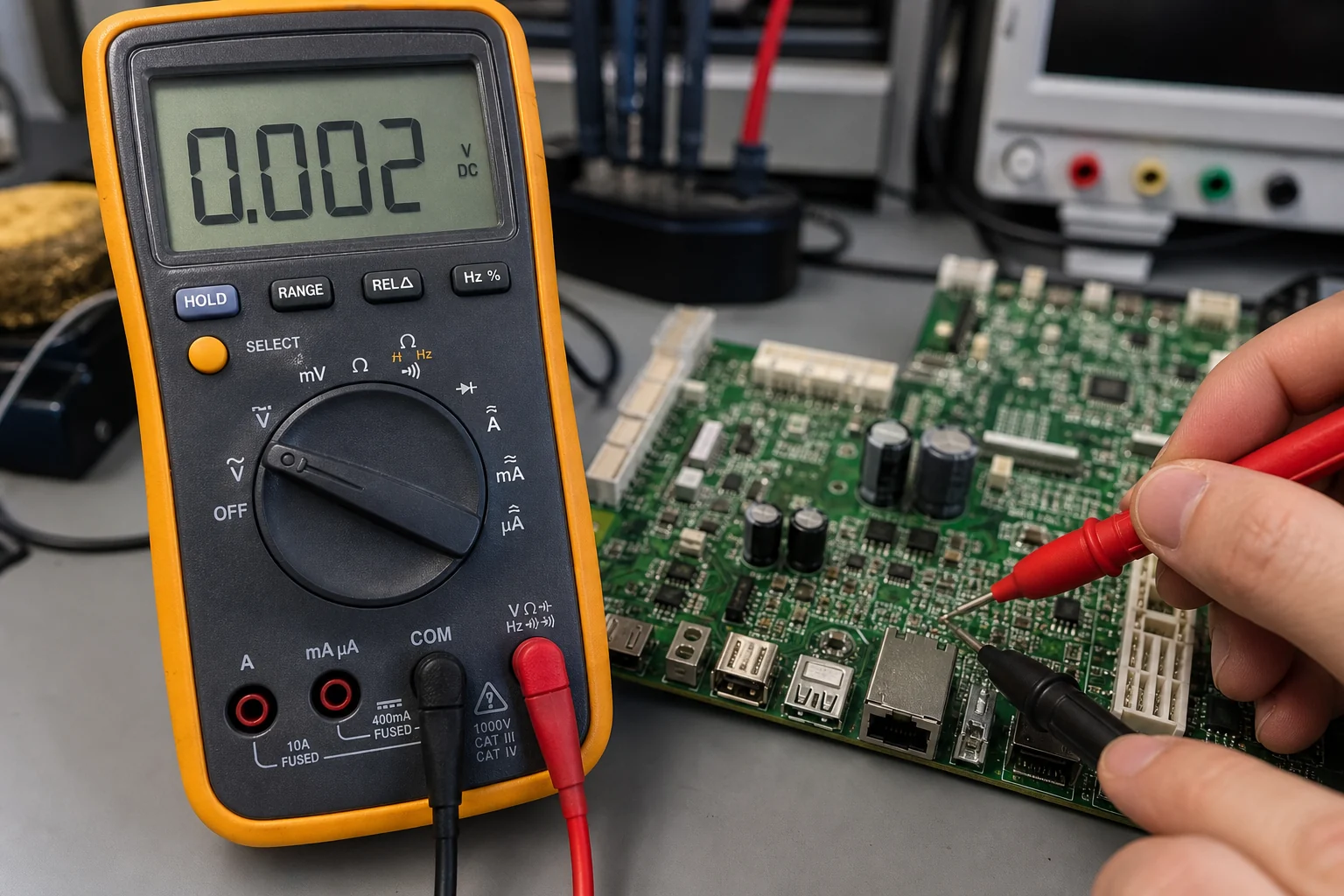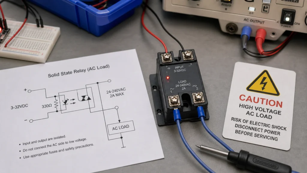
Engineering inquiries regarding the G3MB-202P solid-state relay schematic typically stem from a practical concern: how the compact module actually switches its load, and what parameters require verification before deployment in mains or AC control circuits. Addressing this operational detail is critical, as treating the module as a direct drop-in replacement for a mechanical relay without evaluating its input and output architecture frequently causes circuit failures.
Widely recognized as a compact AC solid-state relay, the G3MB-202P relies on optical isolation paired with a triac-based output topology. Reviewing its schematic provides immediate insight into two crucial aspects: the complete electrical isolation separating the low-voltage control side from the high-voltage AC load side, and the reality that output performance is dictated by load characteristics and switching mechanisms rather than terminal labels alone.
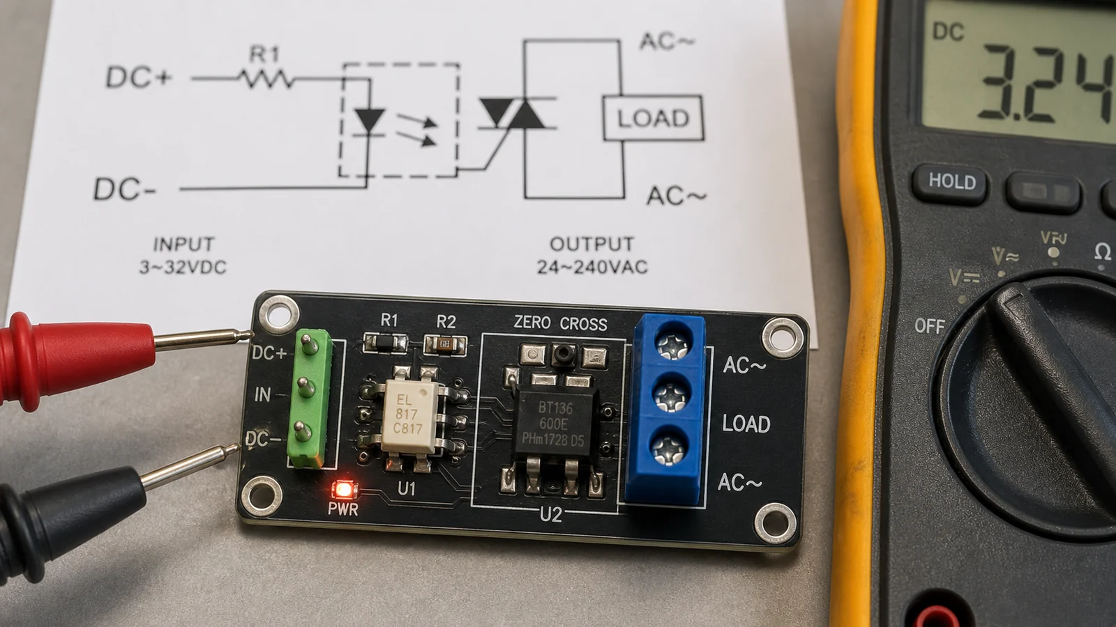
What the schematic is really showing
A typical G3MB-202P schematic separates into two functional blocks. On the control side, a small LED inside an optocoupler is driven from the logic input through a resistor or conditioning network. On the power side, the optical element triggers a triac-based switching structure that controls the AC load. This separation is the core reason solid-state relay modules are useful: the control signal does not drive the load directly, and the low-voltage logic domain is not meant to carry line current.
If you already know the basics from ReversePCB’s general guide to solid-state relays, the next step is learning how the small module implementation changes your assumptions. The module may look simple on a hobby board, but the load path, leakage characteristics, zero-cross behavior, and heat limits still apply.
Why it should not be read like a mechanical relay schematic
Mechanical relays are often drawn as a coil plus contacts. That makes it visually obvious that the output side is physically opening or closing a conductive path. A G3MB-202P style SSR does not behave that way. The output path is semiconductor-based, which means it can have off-state leakage current, voltage drop during conduction, and behavior that depends on whether the load is resistive, inductive, or very small.
This difference is especially important with tiny AC loads, LED lamps, or circuits that do not fully switch off when a little leakage remains. Someone may wire the module correctly and still report that the load glows faintly or behaves unpredictably. The schematic helps explain why: a semiconductor relay output is not a perfect open switch in the same way a clean mechanical contact appears to be.
Input-side checks that prevent common module mistakes
Before looking at the AC side, confirm what the input pin labels really mean on your module version. Some boards are intended for 5 V logic levels, some tolerate 3.3 V drive better than others, and some include indicator LEDs or transistor stages that change the required input current. The safest method is to identify the exact module variant and verify whether the input expects current sourcing, current sinking, or a defined trigger threshold.
It also helps to remember that an optocoupler input is an LED path. If the series resistor value and logic drive are mismatched, the relay may not trigger reliably. A microcontroller pin that barely lights an indicator LED is not the same thing as a verified control stage.
Output-side checks that matter more than the pin names
The AC side is where the biggest misunderstandings appear. The terminal names may tempt people to think in DC terms, but the output device is designed for AC switching behavior. That means the waveform crossing, load type, and surge conditions all matter. A G3MB-202P module may be comfortable with a small resistive load and much less happy with a motor, transformer, or highly reactive device unless the application has been reviewed properly.
Heat is another silent issue. Because the output uses semiconductors, it drops voltage while conducting current. That translates into power dissipation. On a small module, the thermal margin can disappear faster than beginners expect, especially when the board is mounted inside a sealed enclosure with little airflow.
Why the schematic helps when troubleshooting
When a module fails, the schematic tells you where to split the diagnosis. If the logic signal is present but the optocoupler input never sees enough current, the fault is on the control side. If the input is healthy but the load never energizes, the problem may be on the output semiconductor path, the wiring, or the load assumptions. If the load never fully turns off, leakage current or load compatibility may be the real issue rather than a dead part.
This is the same value you get from a structured reading method in ReversePCB’s article on how to read electrical schematics. Once you separate the blocks by function, the module becomes much easier to reason about and much harder to misuse.
Common design mistakes with G3MB-202P modules
The first mistake is trying to use the module as a generic DC relay. The second is ignoring whether the load is inductive, reactive, or too small to behave cleanly with a triac-based output. The third is assuming the module can switch close to its headline rating forever without thermal review. Another common mistake is forgetting board spacing, connector quality, and enclosure safety when the application touches hazardous voltages.
Module convenience does not cancel mains design responsibility. If the board is moving beyond a bench prototype, creepage, clearances, terminals, fuse selection, and enclosure design belong in the conversation.
Where the module fits in real products
G3MB-202P type modules are attractive in thermostats, low-power appliance controls, simple automation outputs, and quick prototypes because they let low-voltage logic control AC devices without mechanical relay noise. That said, good engineering still means matching the module to the load, not matching it to the first online tutorial you find.
If you are designing a custom board around the same function, the schematic also helps you decide whether a module is appropriate at all. In some products a discrete SSR stage or a different switching architecture may provide better thermal performance, better EMC behavior, or better serviceability.
Final takeaway
A G3MB-202P solid-state relay schematic is valuable because it shows the real separation between the control LED path and the AC switching path. Read it that way and the module becomes much easier to use correctly. Ignore that separation and it is easy to make the wrong assumptions about logic drive, load compatibility, leakage current, or thermal margin.
Before wiring one into a product, verify the trigger conditions, the AC load type, the expected current, and the shutdown behavior. Those checks matter far more than the convenience of the three-pin module footprint.
Can a G3MB-202P module switch DC loads the same way it switches AC loads?
No. These modules are commonly intended for AC switching behavior through a triac-based output path. Treating them as generic DC relays is a common mistake.
Why can a load still glow faintly when a solid-state relay is off?
Because semiconductor relay outputs can have off-state leakage current. Small LED or high-impedance loads may react to that leakage even when the relay is not fully on.
Does the schematic tell me whether the module is safe for any mains load?
No. The schematic helps you understand the switching method, but the actual suitability still depends on load type, current, thermal conditions, isolation details, and the full product safety design.
What should I check on the control side first?
Confirm the required input current and logic level for the exact module version so the optocoupler input LED is being driven correctly and repeatably.