Automatización de diseño electrónico (EDA) es la categoría de herramientas de software que los ingenieros utilizan para diseñar, simular y verificar los sistemas electrónicos antes de que se haga una sola placa. Si crees que EDA solo significa «captura esquemática», te estás perdiendo la mayor parte de lo que realmente hacen las cadenas de herramientas EDA modernas. Este artículo explica qué hacen las herramientas para la automatización del diseño electrónico, en qué se diferencian entre sí y qué buscar al elegir una plataforma EDA para el trabajo de PCB.
Lo que realmente cubre la automatización del diseño electrónico
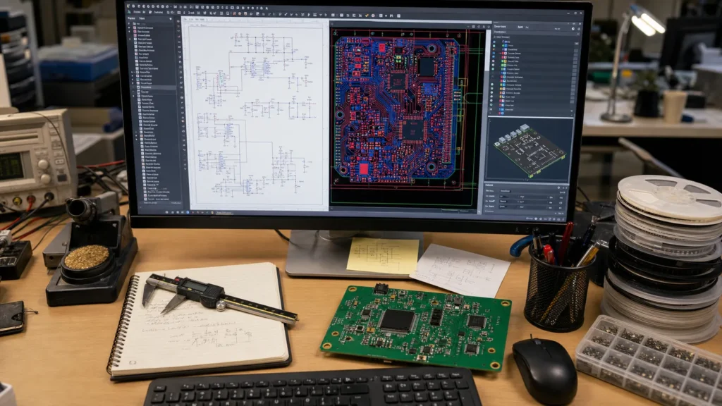
al menos uno Automatización de diseño electrónico Toolchain toma cuatro etapas:
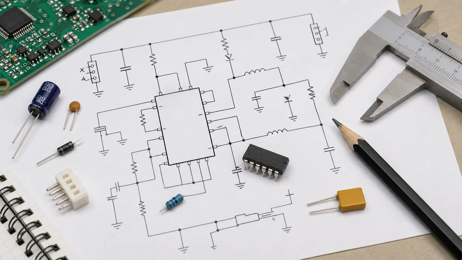
Grabación esquemática: dibujando el circuito lógico. Aquí coloca símbolos, conexiones de cable y asigna valores de componentes. Una buena herramienta de esquema también administra hojas jerárquicas, comprobaciones de reglas de diseño (DRC) y comprobaciones de reglas eléctricas (ERC).
Diseño de PCB: Traducir el diagrama del circuito en una placa física. El editor de PCB coloca huellas, dirige pistas de cobre, define capas de capa y aplica reglas de diseño para compartir, impedancia y capacidad de fabricación.
Simulación y análisis: Simulación SPICE para circuitos analógicos, análisis de integridad de señal para análisis digital de alta velocidad, simulación térmica y PDN (red de distribución de energía). Estos se ejecutan dentro o junto a la herramienta EDA.
Rendimiento de producción: Generación de archivos Gerber, archivos de perforación, datos de pick-and-place y dibujos de ensamblaje. Los errores en esta etapa conducen a los rechazos de fabricación.
Para obtener más información sobre las mejores prácticas esquemáticas, consulte ReversePcbs Guía de diseño de PCBuna
Importantes plataformas EDA para el diseño de PCB
El paisaje de EDA se divide en unos tres niveles, y la elección de los equivocados para su proyecto le causará un verdadero dolor:
| Etapa | instrumentos | mejor para | restricciones |
|---|---|---|---|
| Código abierto / Gratis | Kicad, EasyEDA, LibrePCB | Proyectos de hobby, hardware abierto, tableros de 2-6 capas | Simulación avanzada limitada, gestión de bibliotecas menos robusta |
| Profesional de clase media | Altium Designer, Orcad, Almohadillas | Tableros profesionales de 4 a 16 capas, diseño de alta velocidad, flujos de trabajo en equipo | Costos de suscripción, curva de aprendizaje empinada |
| Empresa / RF especializada | Cadence Allegro, Mentor Xpedition, Vista | Multicapa compleja, HF/Microondas, HDI, Starr-Flex | Costo muy alto, requiere personal de soporte CAD dedicado |
KICAD ha cerrado la brecha con herramientas de gama media para muchos diseños. Ahora es una opción profesional viable para tableros de hasta 8 capas, siempre que su equipo esté familiarizado con el flujo de trabajo de la biblioteca. Cuando diseña una placa digital de alta velocidad con memoria DDR o pares diferenciales de varios GHz, las herramientas de integridad de señal de Altium o Cadence-Level serán más difíciles de reemplazar.
El flujo de trabajo de esquema a PCB en la práctica
Así es como se ve el flujo de trabajo de EDA para un proyecto de PCB típico:
Crea el diagrama de circuito. Coloque iconos, malla de cables, asigne huellas y ejecute el ERC para capturar pines no conectados o salidas en conflicto.
Genera la lista de red. La lista de red es una lista legible por máquina de todos los componentes y conexiones. La herramienta de diseño de PCB lo importa.
Colocar componentes. Coloque las huellas en el contorno del tablero. Agrupe las partes relacionadas, alinee los conectores correctamente y deje espacio para la fijación de agujeros y zonas de sujeción.
trazar pistas. Conecte los pads de acuerdo con la lista de red de acuerdo con las reglas de uso compartido, los requisitos de ancho de pista y los objetivos de impedancia. Las herramientas EDA modernas incluyen el enrutamiento automático, pero las redes críticas siempre deben enrutarse a mano.
Ejecutar Drk. El verificador de reglas de diseño verifica si ningún rastro viola la versión, ningún pad pierde una conexión y cada red se enruta por completo. La existencia del DRK es el requisito mínimo antes de enviar una placa a la fabricación.
Generar archivos de producción. Exporte Gerbers, archivos de perforación NC, listas de materiales y dibujos de ensamblaje. Compruebe el visor Gerber: los errores en esta etapa son caros.
Si se mueve específicamente del diagrama de circuito a la placa de circuito impreso en Altium, Esta guía paso a paso pasa por todo el proceso.
Qué buscar al elegir una herramienta EDA
Concéntrese en lo que realmente afecta su proyecto, no en las características de marketing:
Calidad y gestión de la biblioteca: ¿La herramienta viene con huellas verificadas para los componentes que realmente usa, o pasa horas creando iconos a partir de hojas de datos? Una biblioteca débil pierde más tiempo que cualquier función de simulación que falta.
Funciones de control de diseño: ¿Puede definir reglas por clase de red, par de diferencias y región? Si necesita una impedancia controlada, ¿la herramienta calcula la geometría de rastreo de su apilamiento?
Colaboración: ¿Pueden varios ingenieros trabajar en el mismo proyecto? ¿Soporta el control de versiones? La integración de Git se está volviendo cada vez más estándar en las herramientas modernas de EDA.
Confiabilidad del rendimiento de fabricación: ¿Las exportaciones de Gerber coinciden con el tablero? Algunas herramientas aplican tácitamente correcciones de reglas de diseño que cambian la placa durante la salida. Revise en un visor Gerber cada vez.
Integración de simulación: Si confía en la simulación de Spice, ¿la herramienta lo integra de forma nativa o necesita exportar netlists a un simulador externo?
Errores comunes de EDA que logran la fabricación
Redes inquietas que cruzan la República Democrática del Congo: Algunas herramientas permiten que las redes no enrutadas entreguen el DRC cuando se marquen como «sin conexión». Compruebe cada red visualmente o con un informe de conectividad.
PIN 1 DE HUELLA DESAPARECIMIENTO: El símbolo esquemático y la huella de PCB no están de acuerdo con la alineación del pin 1. Esta es la causa más común de fallas en la primera placa de revisión. Compruebe siempre la pantalla PIN-1 en cada huella de IC.
Almohadillas de impresión de pantalla superpuestas: Serigrafía en almohadillas de cobre evita la soldadura. La mayoría de las herramientas tienen una regla de limpieza de pantalla a almohadilla – activarlas.
Impedancia insuperable: La geometría de traza en el diseño no genera la impedancia de destino porque el apilamiento se definió incorrectamente en la herramienta. Compruebe la impedancia con el apilamiento de IST del procesador, no la herramienta estándar.
Preguntas frecuentes
¿Qué es la automatización del diseño electrónico?
Electronic Design Automation (EDA) es una categoría de software de desarrollo de sistemas electrónicos, que incluye captura esquemática, diseño de placa de circuito, simulación de circuitos y generación de archivos de fabricación. Las herramientas EDA son esenciales para el desarrollo de placas de circuitos modernos.
¿Kicad es lo suficientemente bueno para el diseño profesional de PCB?
Sí, KICAD ahora puede crear un diseño de tablero profesional para tableros de hasta 8 capas. Admite enrutamiento de pares diferenciales, ajuste de longitud y visualización 3D. Para diseños muy rápidos que requieren simulación avanzada de integridad de señal, las herramientas de Altium o Cadence proporcionan un análisis más profundo.
¿Cuál es la diferencia entre la grabación esquemática y el diseño de PCB?
La captura esquemática es la fase de diseño lógico en la que se definen las conexiones de los componentes y los circuitos. El diseño de PCB es la fase de diseño físico en la que se colocan los componentes, coloca las pistas de cobre y prepara la placa para la fabricación.
¿Necesito una simulación en mi herramienta EDA?
La simulación es opcional para tableros digitales simples. Para circuitos analógicos, fuentes de alimentación o diseños digitales de alta velocidad, la simulación SPICE y el análisis de integridad de la señal detectarán los problemas antes de fabricar y almacenar rotaciones de revisión.
¿Qué archivos genera una herramienta EDA para la fabricación?
Las salidas de fabricación estándar incluyen archivos Gerber (formato RS-274X o X2) para cada capa de cobre, máscara de soldadura y serigrafía; Archivos de perforación NC; Archivos de pick-and-place automáticos de montaje; y una bom (bom).