Электронная автоматизация проектирования (EDA) — это категория программных инструментов, которые инженеры используют для проектирования, моделирования и проверки электронных систем до того, как будет изготовлена одна печатная плата. Если вы думаете, что EDA просто означает «схема захвата», вы упускаете большую часть того, что на самом деле делают современные цепочки инструментов EDA. В этой статье объясняется, что делают электронные инструменты автоматизации дизайна, чем они отличаются друг от друга и на что обращать внимание при выборе платформы EDA для работы PCB.
Что на самом деле охватывает электронная автоматизация дизайна
Как минимум, Электронная автоматизация проектирования Инструментальная цепочка обрабатывает четыре этапа:
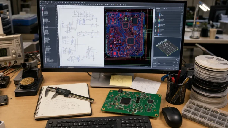
Схематический захват: рисование логической схемы. Здесь вы размещаете символы, проводные соединения и присваиваете значениям компонентам. Хороший инструмент схемы также управляет иерархическими листами, проверками правил проектирования (DRC) и электрическими проверками правил (ERC).
Компоновка печатной платы: перевод схемы на физическую плату. Редактор печатной платы размещает следы, направляет медные трассы, определяет плоские слои и применяет правила проектирования для очистки, импеданса и технологичности.
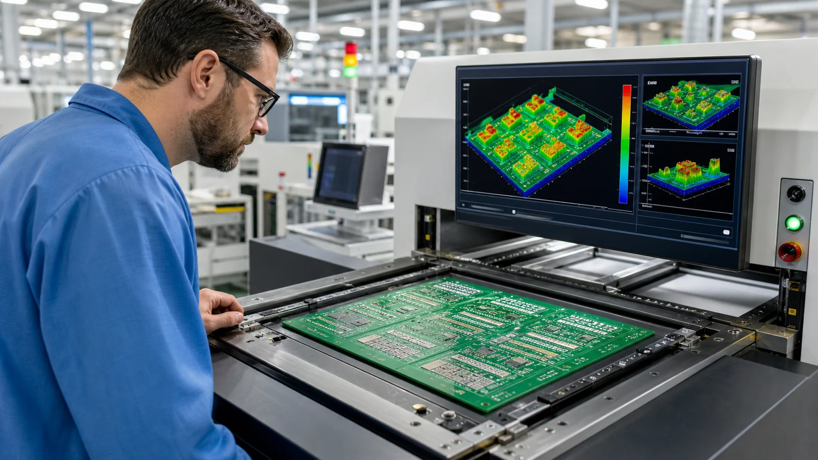
Моделирование и анализ: имитация SPICE для аналоговых схем, анализ целостности сигнала для высокоскоростного цифрового моделирования и анализа сети распределения электроэнергии (PDN). Они работают внутри или рядом с инструментом EDA.
Производственные результаты: генерация файлов Gerber, файлы сверла, данные сборки и сборки и сборочные чертежи. Ошибки на данном этапе создают отвержения производства.
Более подробную информацию о схематических практиках см. Руководство по проектированию печатных плат ReversePCB.
Основные платформы EDA для дизайна печатных плат
Пейзаж EDA разделяется примерно на три уровня, и выбор неправильного для вашего проекта вызывает настоящую боль:
| Ярус | Инструментарий | лучше всего для | Недостатки |
|---|---|---|---|
| Открытый исходный / бесплатный | Kicad, Easyeda, LibrePCB | Хоббиистские проекты, открытое оборудование, 2-6 слоёв | Limited advanced simulation, less robust library management |
| Профессионал среднего класса | Altium Designer, Orcad, прокладки | Профессиональные 4-16-слойные доски, высокоскоростной дизайн, рабочие процессы команды | Стоимость подписки, крутая кривая обучения |
| Предприятие / RF-специализировано | Cadence Allegro, Mentor Xpedition, реклама | Комплексный многослойный, RF/Microwave, HDI, жестко-гибкий | Очень высокая стоимость, требуется специальный вспомогательный персонал САПР |
KICAD закрыла пробел с помощью инструментов среднего класса для многих дизайнов. В настоящее время это жизнеспособный профессиональный выбор для плат до 8 уровней, если ваша команда будет комфортно работать с библиотечным рабочим процессом. Если вы разрабатываете высокоскоростную цифровую плату с памятью DDR или дифференциальными парами на нескольких ГГц, инструменты целостности сигнала Altium или Cadence-уровня становятся труднее заменить.
Рабочий процесс схемы к печатной плате на практике
Вот как выглядит рабочий процесс EDA для типичного проекта печатной платы:
Создайте схему. Поместите символы, проводные сети, назначьте следы и запустите ERC, чтобы ловить неподключенные контакты или противоречивые выходы.
Сгенерируйте список сетей. NetList — это машиночитаемый список каждого компонента и соединения. Инструмент компоновки печатных плат импортирует его.
Поместите компоненты. Поместите следы на контуре доски. Группируйте связанные детали, правильно ориентируйте соединители и оставьте место для монтажных отверстий и зон для выдержки.
Следы маршрута. Соединяйте пэды в соответствии с списком сетей, соблюдая правила очистки, требования к ширине трассировки и целевые показатели импеданса. Современные инструменты EDA включают автоматическую маршрутизацию, но критические сети всегда должны быть направлены вручную.
запустить ДРК. Проверка правил проектирования проверяет, что ни одна трассировка не нарушает зазор, ни в одной площадке не отсутствует соединение, и каждая сеть полностью маршрутизируется. Прохождение DRC является минимальным требованием перед отправкой платы на изготовление.
Сгенерировать производственные файлы. Экспортируйте Gerbers, NC Drill Files, BOM и сборочные чертежи. Дважды проверьте Gerber Viewer — ошибки на данном этапе стоят дорого.
Если вы переходите от схемы к печатной плате в Altium, Это пошаговое руководство Проходит полный процесс.
На что обратить внимание при выборе инструмента EDA
Сосредоточьтесь на том, что на самом деле влияет на ваш проект, а не на маркетинг подсчета функций:
Качество и управление библиотекой: поставляется ли инструмент с проверенными следами для компонентов, которые вы действительно используете, или вы будете часами создавать символы из технического описания? A weak library wastes more time than any missing simulation feature.
Возможности правила проектирования: можете ли вы определить правила по классу net, дифференциальной паре и региону? Если вам нужен контролируемый импеданс, инструмент вычисляет геометрию трассировки из вашего стека?
Сотрудничество: могут ли несколько инженеров работать над одним и тем же проектом? Поддерживает ли он контроль версий? Интеграция Git становится все более стандартной в современных инструментах EDA.
Надежность производства: Соответствует ли экспорт Gerber экспорту платы в соответствии с проектом? Некоторые инструменты бесшумно применяют исправления правил проектирования во время вывода, которые меняют плату. Каждый раз проверяйте в Gerber Viewer.
Интеграция с моделированием: если вы полагаетесь на моделирование SPICE, интегрирует ли инструмент изначально или вам нужно экспортировать списки сетей во внешний симулятор?
Распространенные ошибки EDA, которые доходят до изготовления
Немаршрутизированные сети, проходящие мимо DRC: некоторые инструменты позволяют ненаправленным сетям передать DRC, если они помечены как «без подключения». Визуально проверяйте каждую сеть или с помощью отчета о подключении.
PIN-код 1 Несоответствие: Схематический символ и след печатной платы не согласны с ориентацией контакта 1. Это наиболее частая причина сбоев платы первой ревизии. Всегда визуально проверяйте индикаторы контакта 1 на каждом следе IC.
Накладки из шелкографии: шелкография, напечатанная на медных прокладках, предотвращает пайку. Большинство инструментов имеют правило очистки шелкографией к прокладке — включите его.
Непревзойденное импеданс: геометрия трассировки в макете не создает целевое сопротивление, поскольку в инструменте установлено неправильное определение. Проверьте импеданс с фактическим стеком производителя, а не по умолчанию инструмента.
Часто задаваемые вопросы
Что такое электронная автоматизация дизайна?
Электронная автоматизация проектирования (EDA) — это категория программного обеспечения, используемая для проектирования электронных систем, включая схему захвата, компоновку печатных плат, моделирование схем и генерацию файлов. Инструменты EDA необходимы для современной разработки печатных плат.
Достаточно ли KICAD для профессионального дизайна печатных плат?
Да, теперь KiCad способен печатать печатную плату профессионального уровня для плат до 8 слоев. Он поддерживает маршрутизацию дифференциальной пары, длинную настройку и 3D-визуализацию. Для высокоскоростных конструкций, требующих расширенного моделирования целостности сигнала, инструменты Altium или Cadence обеспечивают более глубокий анализ.
В чем разница между схематическим захватом и компоновкой печатной платы?
Схематический захват — это фаза логического проектирования, где вы определяете соединения компонентов и функцию схемы. Компоновка печатной платы — это фаза физического проектирования, где вы размещаете компоненты, направляете медные следы и готовите плату к производству.
Нужно ли мне моделирование в моем инструменте EDA?
Для простых цифровых плат моделирование не является обязательным. Для аналоговых схем, блоков питания или высокоскоростных цифровых конструкций, моделирования SPICE и анализа целостности сигналов перед изготовлением и сохранением вращений.
Какие файлы генерирует инструмент EDA для производства?
Стандартные производственные выходы включают файлы Gerber (формат RS-274X или X2) для каждого медного слоя, припой и шелкографии; Файлы сверла ЧПУ; Файлы Pick-and-Place (Centroid) для автоматической сборки; и чек материалов (BOM).