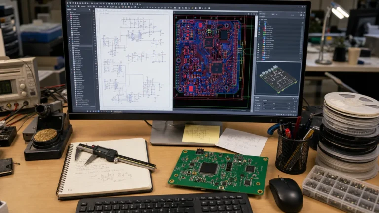
elektronik tasarım otomasyonu (EDA), yazılım mühendislerinin tek bir PCB oluşturulmadan önce elektronik sistemleri tasarlamak, simüle etmek ve doğrulamak için kullandıkları bir kategoridir. EDA’nın yalnızca “şematik alma” anlamına geldiğini düşünüyorsanız, modern EDA araç zincirinin gerçekte yaptığı şeylerin çoğunu kaybedersiniz. Bu makale, elektronik tasarım otomasyon araçlarının birbirlerinden nasıl farklı olduklarını ve PCB çalışmaları için bir EDA platformu seçerken nelere dikkat etmeleri gerektiğini açıklar.
Elektronik tasarım otomasyonu gerçekte ne içerir?
En azından bir elektronik tasarım otomasyonu Araç zinciri dört aşamayı işler:
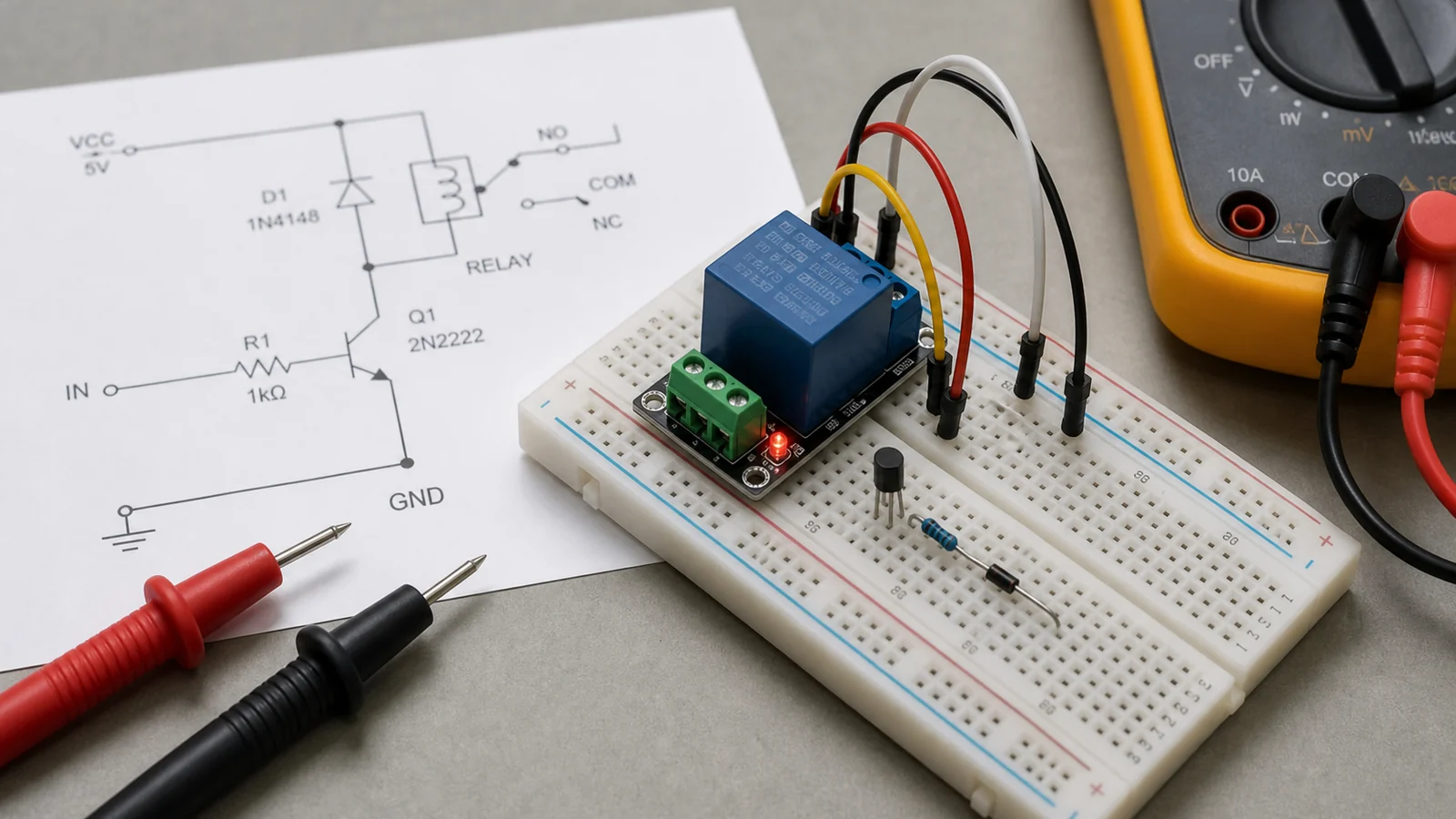
Şema Alma: Mantıksal bir devre çizin. Sembolleri, kablo bağlantılarını ve bileşen değerlerini ayarladığınız yer burasıdır. İyi şematik araçlar ayrıca hiyerarşik sayfaları, tasarım kurallarını (DRC) ve elektrik kurallarını (ERC) kontrol etmeyi de yönetir.
PCB düzeni: Şemayı fiziksel tahtaya çevirin. PCB editörü ayak izleri, bakır iz yolları yerleştirir, alanın katmanlarını tanımlar ve izinler, empedans ve üretim yetenekleri için tasarım kurallarını uygular.
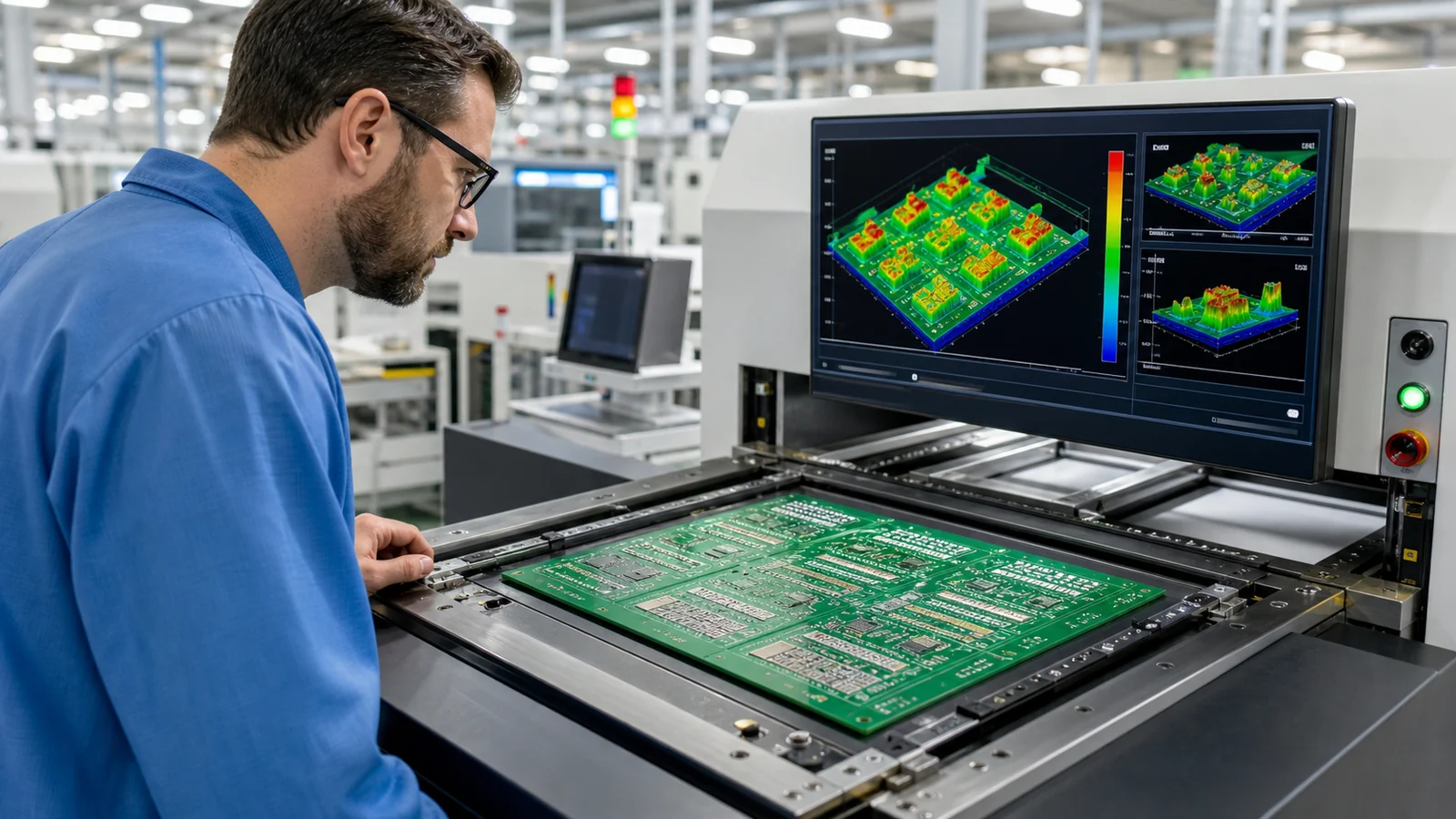
Simülasyon ve Analiz: Analog devre için SPICE simülasyonu, yüksek hızlı dijital analiz, termal simülasyon ve güç dağıtım ağı (PDN) için sinyal bütünlüğü analizi. EDA aracının içinde veya yanında çalışır.
üretim gücü: Gerber dosyaları, matkap dosyaları, toplama ve yerleştirme verileri ve montaj görüntüleri oluşturur. Bu aşamadaki hatalar, imalatın reddedilmesini sağlar.
Şematik en iyi uygulamalar hakkında daha fazla bilgi için bkz. Kılavuz reversePCB’ler PCB şematik tasarımı.
PCB tasarımı için ana EDA platformu
EDA manzarası kabaca üç seviyeye ayrılmıştır ve projeniz için yanlış olanı seçmek gerçek bir acıya neden olur:
| Seviye | Araç | en iyisi | Sınırlama |
|---|---|---|---|
| Açık/serbest kaynak | Kicad, EasyEda, LibePCB | Hobi projesi, açık donanım, 2-6 katmanlı pano | Sınırlı gelişmiş simülasyon, daha az güçlü kütüphane yönetimi |
| Orta sınıf profesyoneller | Altium Designer, OrCAD, PADS | Profesyonel 4-16 katmanlı tahta, yüksek hızlı tasarım, takım iş akışı | Abonelik ücreti, dik öğrenme eğrisi |
| Şirket / RF-uzmanlaştırma | Cadence Allegro, Mentor Xpedition, ADS | Çok Katmanlı Kompleks, RF/Mikrodalga, HDI, Rijit-Flex | Çok yüksek maliyet, özel CAD destek personeli gerektirir |
KICAD, birçok tasarım için orta menzilli bir araçla boşluğu kapattı. Ekibinizin kütüphane iş akışında rahat olması koşuluyla, artık yaklaşık 8 katmana kadar olan panolar için uygun bir profesyonel seçimdir. Bazı GHz’de DDR bellek veya diferansiyel eşleştirme ile yüksek hızlı bir dijital kart tasarlıyorsanız, Altium Sinyal Bütünlüğü Aracı veya ritim seviyesinin değiştirilmesi daha zor hale gelir.
Uygulamada Şematik-PCB iş akışı
İşte normal bir PCB projesi için EDA iş akışının görünümü:
Şema Oluştur. Bağlantısız pinleri veya çakışan çıktıları yakalamak için semboller yerleştirin, tel örgü, ayak izleri ayarlayın ve ERC’yi çalıştırın.
netlist oluştur. NetList, her bileşenin ve bağlantının makine tarafından okunabilen bir listesidir. PCB düzen aracı bunu içe aktarır.
Bileşenleri yerleştirin. Ayak izlerini tahtanın ana hatlarına yerleştirin. İlgili parçaları gruplandırın, konektörleri doğru bir şekilde işaretleyin ve delikler ve depolama bölgeleri için yer bırakın.
rota izi. Rulmanları netlist’e göre bağlayın, izin kurallarına, iz genişliği gereksinimlerine ve empedans hedeflerine uyun. Modern EDA araçları otomatik yönlendirmeyi içerir, ancak kritik ağlar her zaman elle yönlendirilmelidir.
DRC’yi çalıştır. Tasarım kuralı denetleyicisi, izinleri ihlal eden hiçbir iz olmadığını, hiçbir pedin eksik bağlantıları olmadığını ve her ağın tamamen yeniden yönlendirildiğini doğrular. DRC’yi geçmek, tahtayı imalata göndermeden önce minimum gerekliliktir.
üretim dosyaları oluştur. Gerberleri, NC matkap dosyalarını, bombaları ve montaj çizimlerini dışa aktarın. Gerber görüntüleyiciyi tekrar kontrol edin – bu aşamadaki hata pahalıdır.
Özellikle Altium’da şematikten PCB’ye geçerseniz, kılavuz bu adım adım tam bir süreçten geçmek.
EDA araçlarını seçerken nelere dikkat edilmelidir?
Özelliklerin sayısını pazarlamaya değil, projenizi gerçekte neyin etkilediğine odaklanın:
Kütüphane kalitesi ve yönetimi: Bu araç, gerçekten kullandığınız bileşenler için doğrulanmış izlerle donatılmış mı, yoksa veri sayfalarından semboller oluşturmak için saatler harcayacak mısınız? Zayıf kitaplıklar, eksik simülasyon özelliklerinden daha fazla zaman harcar.
tasarım kuralları yeteneği: Kuralları temiz sınıf, diferansiyel çifti ve bölgeye göre belirtebilir misiniz? Kontrollü empedansa ihtiyacınız varsa, araç yığınınızın izleme geometrisini hesaplar mı?
İşbirliği: Birden fazla mühendis aynı projede çalışabilir mi? Sürüm kontrolünü destekliyor mu? Git entegrasyonu, modern EDA araçlarında giderek daha standart hale geliyor.
Üretim çıkış güvenilirliği: Gerber’in ihracatı tasarlanan kartla eşleşiyor mu? Bazı araçlar, panoyu değiştiren çıktı sırasında tasarım kurallarının düzeltilmesini gizlice uygular. Gerber Viewer’da her zaman doğrulayın.
Simülasyon entegrasyonu: SPICE simülasyonuna güveniyorsanız, araç onu yerel olarak entegre ediyor mu, yoksa bir NetList’i harici bir simülatöre dışa aktarmanız mı gerekiyor?
İmalat sağlayan EDA’nın yaygın hataları
DRC’yi geçmeyen ağlar: Bazı araçlar, “Bağlantı Yok” olarak işaretlenirse DRC’yi atlamak için yönlendirilmeyen ağlara izin verir. Her ağı görsel olarak veya bir bağlantı raporuyla doğrulayın.
Ayak İzi Pin 1 Uyumsuzluk: Şematik semboller ve PCB izleri PIN oryantasyonunda aynı fikirde değil 1. Bu, ilk revizyon kartının başarısızlığının en yaygın nedenidir. Her IC izlemede her zaman PIN 1 göstergesini görsel olarak doğrulayın.
serigrafi örtüşen rulmanlar: Bakır pedlere basılmış serigrafi lehimlemeyi önler. Çoğu araç, serigrafiden pede izin kurallarına sahiptir – Etkinleştir.
Eşsiz Empedans: Düzendeki geometri izleri, yığın araçta yanlış tanımlandığından hedef empedansı oluşturmaz. Varsayılan araçla değil, gerçek imalatçı yığınıyla empedansı doğrulayın.
Sıkça Sorulan Sorular
elektronik tasarım otomasyonu nedir?
Elektronik Tasarım Otomasyonu (EDA), şematik yakalama, PCB düzeni, devre simülasyonu ve üretim dosyası oluşturma dahil olmak üzere elektronik sistemler tasarlamak için kullanılan bir yazılım kategorisidir. EDA araçları, modern PCB geliştirme için gereklidir.
KICAD, profesyonel PCB tasarımı için yeterince iyi mi?
Evet, KICAD artık yaklaşık 8 katmana kadar olan kartlar için profesyonel sınıf PCB’ler tasarlama yeteneğine sahiptir. Diferansiyel çift yönlendirme, uzun ayarlama ve 3D görselleştirmeyi destekler. Gelişmiş sinyal bütünlüğü simülasyonu gerektiren çok yüksek hızlı tasarım için altium veya ritim araçları daha derin analiz sağlar.
Şematik yakalama ve PCB düzeni arasındaki fark nedir?
Yakalama şeması, bileşenlerin ve devre fonksiyonlarının bağlantısını belirlediğiniz mantıksal bir tasarım aşamasıdır. PCB düzeni, bileşenleri yerleştirdiğiniz, bakır izlerini yönlendirdiğiniz ve üretim için levhalar hazırladığınız fiziksel bir tasarım aşamasıdır.
EDA aracımda bir simülasyona ihtiyacım var mı?
Basit bir dijital kart için simülasyon isteğe bağlıdır. Analog devreler, güç kaynağı veya yüksek hızlı dijital tasarım için, baharat simülasyonu ve sinyal bütünlüğü analizi, üretimden önce sorunları yakalayın ve revizyon turlarından tasarruf edin.
EDA aracı üretim için hangi dosyaları üretir?
Standart üretim çıktısı, her bakır tabakası, lehim maskesi ve serigrafi için Gerber dosyasını (RS-274X veya X2 formatı) içerir; NC dosya matkabı; otomatik montaj için topla ve yerleştir (merkez) dosyası; ve malzeme faturaları (BOM).