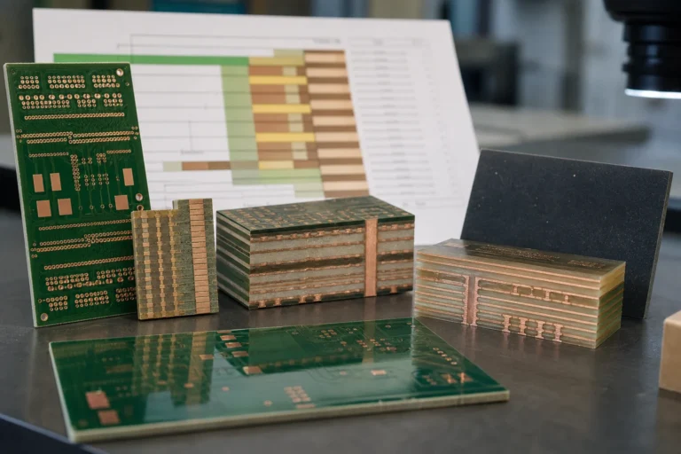
A Standard PCB Stackup Stops Being Standard When Yield, EMI, and Cost Pull Apart
Standard 2-, 4-, 6-, and 8-layer PCB stackups only work when return paths, impedance, copper balance, and fabrication assumptions still match the real design.

Standard 2-, 4-, 6-, and 8-layer PCB stackups only work when return paths, impedance, copper balance, and fabrication assumptions still match the real design.
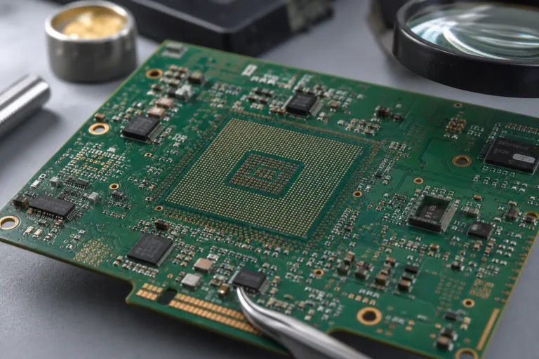
Via in pad can solve dense BGA and QFN escape problems, but only when fill, cap, planarity, paste behavior, and inspection risk are reviewed before release.
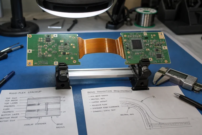
A rigid-flex PCB stackup is not just a layer list. It sets bend reliability, copper strain, stiffener transitions, impedance behavior, and assembly risk long before fabrication starts.
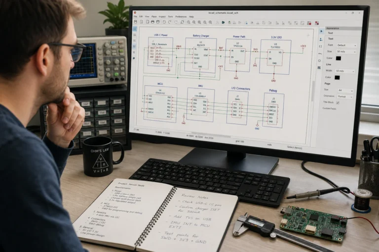
If you want to create a KiCad design from text, start with structured parts, named nets, power assumptions, and ERC checks so the generated schematic stays editable and reviewable.
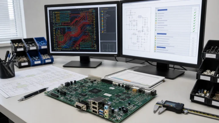
Moving a legacy Protel design into Altium Designer is not just a file-open task. This guide covers libraries, rules, polygons, outputs, and verification steps that keep old boards manufacturable after migration.
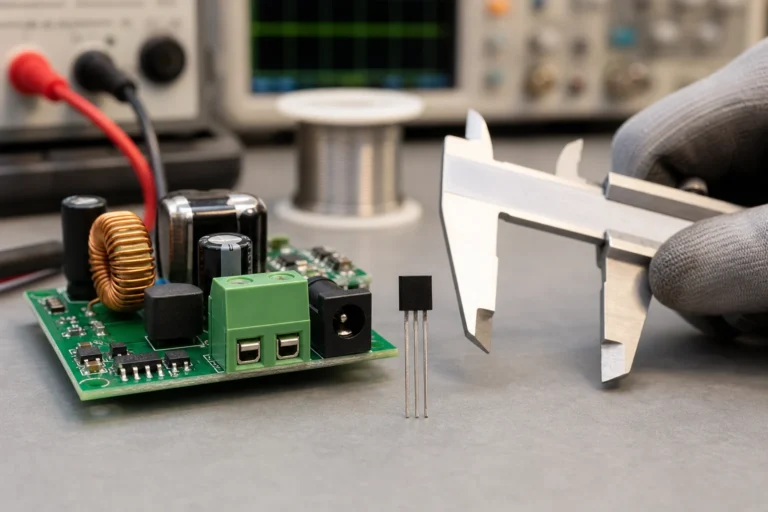
Choosing the smallest N-channel MOSFET through hole package means balancing gate drive, fault energy, thermal margin, pinout, and rework access on the real PCB.
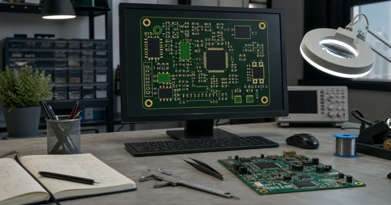
Learn how to fix KiCad silkscreen-to-mask clearance warnings without hiding real DFM issues. Start at the footprint, verify Gerbers, and protect assembly-critical legend.
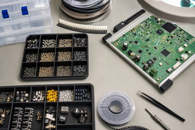
Surface mount components are the parts soldered directly onto PCB pads, but the useful question is how their packages affect placement, reflow, inspection, and rework. This guide explains the main SMT component families and the assembly risks each one introduces.
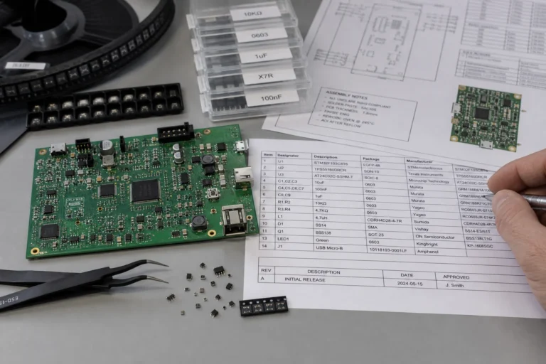
SMD and SMT are closely related, but they do not mean the same thing. This guide explains the difference between the component and the manufacturing process, where each term belongs in PCB documentation, and why mixing them up creates assembly mistakes.
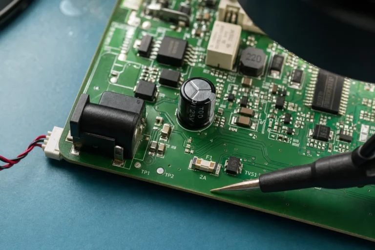
An SMT fuse can protect a PCB only if its interrupt rating, I2t, package, and placement match the real fault path. This guide explains how to choose, place, inspect, and troubleshoot a surface-mount fuse in power-input and subsystem designs.
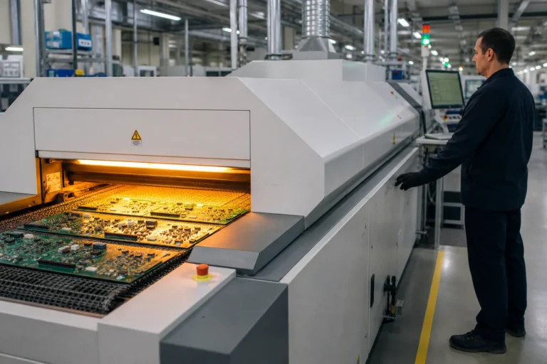
A reflow machine is only one part of a stable SMT process. This guide explains what the machine controls, which profile variables matter most, and why board design, paste deposition, and package mix still determine whether reflow stays repeatable.
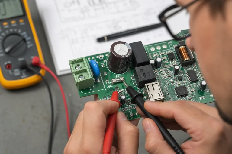
An SMT fuse is a small component with system-level consequences. This guide explains how current rating, inrush, fault energy, layout heat, and service access shape the right fuse choice on a PCB.