Choosing a small through-hole N-channel MOSFET involves balancing tight PCB space against thermal and power handling limits. While minimal packages like TO-92 fit density-constrained layouts, they offer limited thermal margin and restricted Safe Operating Area (SOA). A successful design prioritizes a package that meets physical space constraints without compromising gate drive margins or long-term circuit reliability.
Start with the fault path, not the package outline
A small through-hole MOSFET is often placed near a connector, battery input, relay coil, or low-side load. In each case, the failure condition matters more than the nominal load current. A motor stall, an input short, or an inductive turn-off event can demand far more from the MOSFET than the normal operating point.
Check the drain-source voltage against the supply plus credible transients, then check the safe-operating-area graph for the switching or linear condition the circuit can actually create. A MOSFET that looks comfortable at a steady 300 mA load may not be comfortable while charging a capacitive input, clamping a relay transient, or dissipating energy during a slow gate transition.
Why the smallest package can become the hottest part
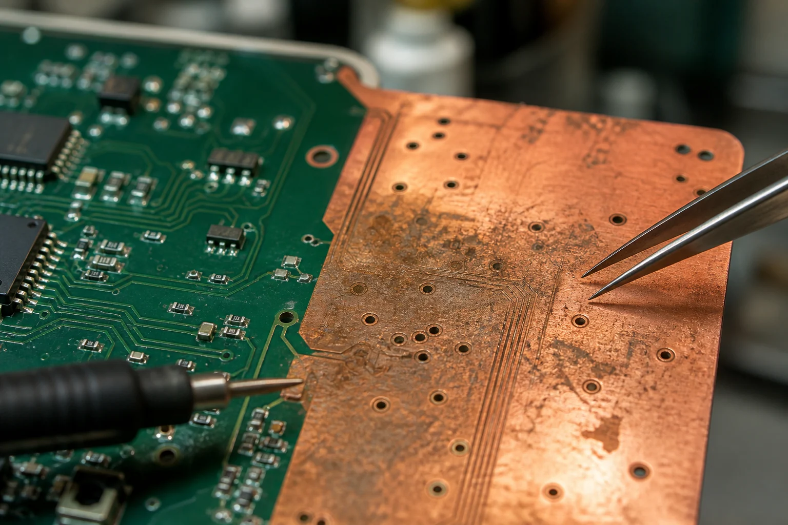
Compact through-hole packages have limited die area and limited thermal paths. The leads conduct some heat into the board, but a small board, narrow copper, or a vertical installation can leave the device with much less cooling than a datasheet test condition suggests. Treat the quoted thermal resistance as a starting point, not a board-level guarantee.
Estimate conduction loss from the on-resistance at the gate voltage and temperature you will use, then add switching loss where the MOSFET changes state frequently. Logic-level behavior is especially easy to misread: an attractive on-resistance may be specified at a higher gate voltage than a 3.3 V controller can provide. For a low-side switch driven directly from a microcontroller, verify the relevant curves or guaranteed values at the real gate drive.
Package size is only one of the fit checks
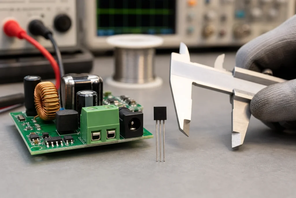
TO-92 and similar small packages are attractive because they use little board area and are easy to hand-solder. Their limitations show up when current, ambient temperature, or switching speed rises. A larger through-hole package may consume more room but offer a better lead frame, more useful copper coupling, and a serviceable thermal path. The right comparison is the completed assembly, not just the body dimensions in the distributor table.
Pinout and footprint are not interchangeable
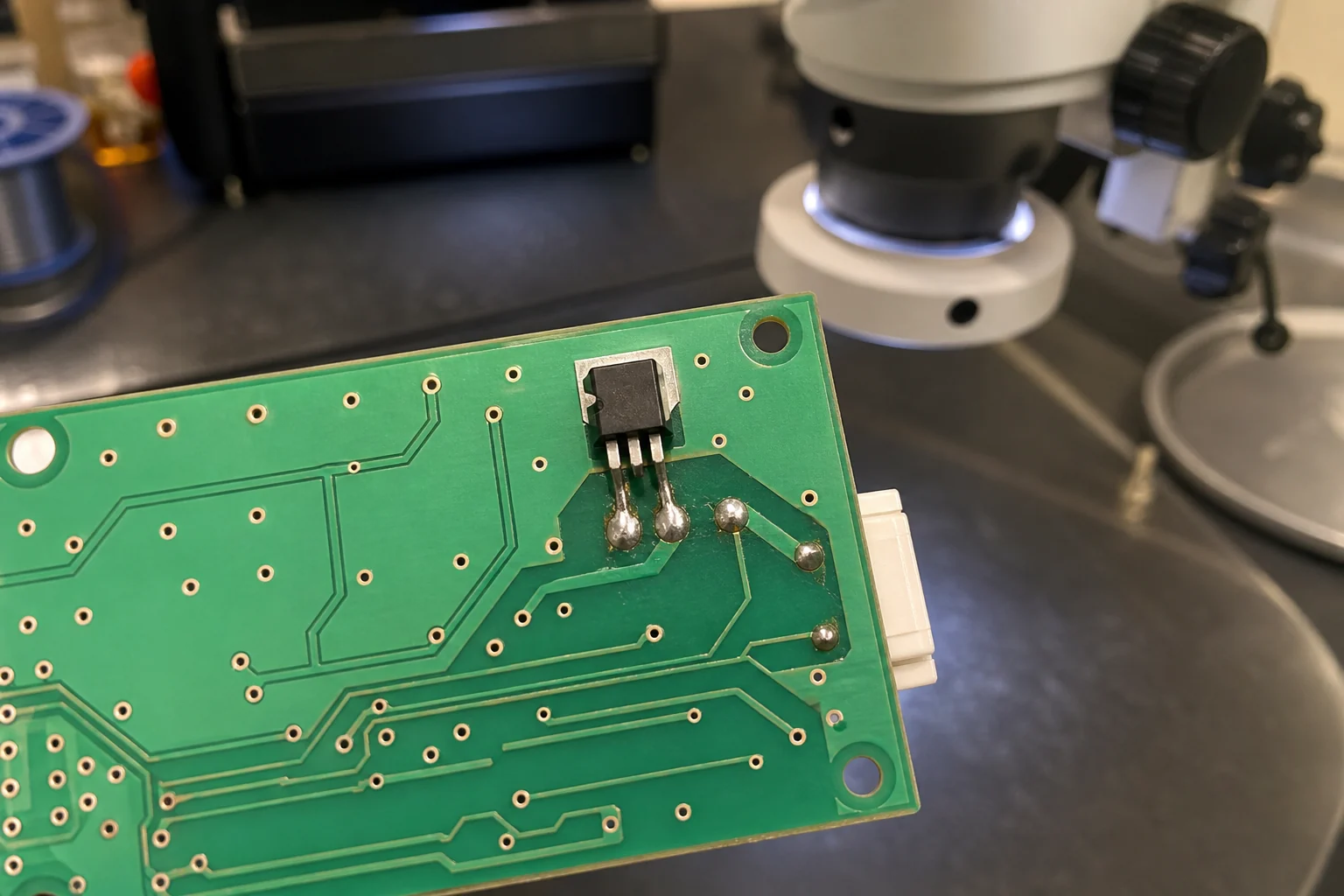
Parts with the same outline can use different gate, drain, and source lead order. Do not reuse a footprint only because the body looks familiar. Check the manufacturer drawing, make the symbol-to-footprint mapping explicit, and keep enough lead clearance to avoid stressing the package during insertion or rework. That same discipline applies when deciding between through-hole and surface-mount choices for a product that may need field repair.
Leave a realistic rework path
A small MOSFET next to a tall connector or electrolytic capacitor can be electrically correct and still be difficult to replace without damaging the board. Leave iron access around the leads, avoid using the device lead as the only high-current thermal path, and keep sensitive plastic parts outside the likely rework heat zone. These choices matter most on low-volume controllers, power-entry boards, and serviceable industrial assemblies.
A practical selection sequence
Define the normal current, fault current, switching frequency, and drain-source voltage including transients.
Confirm the guaranteed on-resistance at the available gate voltage, not only the headline maximum rating.
Estimate loss at hot conditions and compare it with the assembled board’s available copper and airflow.
Check the safe-operating-area and avalanche guidance when the load is inductive or a control fault can leave the part partly on.
Verify pinout, drilling, lead spacing, insertion clearance, and the rework path with the actual mechanical parts nearby.
Build a representative board and measure drain-source voltage, gate voltage, and case temperature at the worst expected load before freezing the BOM.
When a through-hole MOSFET is still the better choice
Through-hole devices remain sensible when the product needs manual assembly, repairable power switching, a modest production volume, or a package that can tolerate straightforward field rework. They are less attractive when board height is constrained, switching loss is significant, or the thermal budget depends on a large copper pad. In those cases, a properly designed surface-mount footprint may deliver lower resistance and a more predictable heat path.
The smallest part should still leave margin
The smallest N-channel MOSFET through hole option is a valid starting point for a compact, low-power design. It is not a selection rule. Choose the package after the circuit has a defined gate drive, transient strategy, thermal path, and service requirement. A little extra package and copper area is often cheaper than a marginal switch that only fails after the enclosure warms up.
FAQ
What is the smallest common through-hole package for an N-channel MOSFET?
TO-92-style packages are commonly used for compact through-hole MOSFET designs, but the smallest useful option depends on voltage, current, gate drive, and thermal margin. A smaller body does not automatically mean a suitable power switch.
Can a 3.3 V microcontroller drive a small N-channel MOSFET directly?
Only if the selected part has suitable on-resistance performance at the actual 3.3 V gate drive and the switching conditions are within its limits. Check guaranteed specifications and curves rather than assuming every logic-level MOSFET behaves the same.
Why does a small through-hole MOSFET run hot at a modest load?
Heat can come from on-resistance at the actual junction temperature, slow switching, limited copper area, poor airflow, or current and transient conditions that are higher than the nominal load suggests. Measure the assembled board under a representative worst case.
Should I choose through-hole or surface-mount for a MOSFET?
Choose through-hole when serviceability, manual assembly, and mechanical access matter. Choose surface-mount when low profile, lower resistance, or a large copper thermal pad is more important. The decision should follow the board’s electrical and manufacturing constraints.