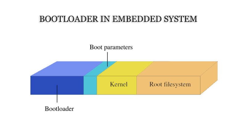
Bootloaders Explained: How They Start Devices
What’s a bootloader? Learn firmware initialization, update processes, and compatibility with Arduino/STM32. Critical for embedded system startups. Guide here!
Schematic & Gerber restoration
MCU/CPLD code restore access & backup
1:1 exact hardware replication
BLE & Classic BT wireless solutions
Precision PID & thermal management
High-efficiency motor drive control
Industrial RS485/RTU communication
Custom STM32/ESP32 firmware & HW
Calculate the PCB trace width based on temperature rise, current, and copper thickness (IPC-2152).
Learning from our posts in different topics: development case of chips, reverse engineering applications, ic programming tutorials, and more. Our team of experienced PCB experts are here to answer your queries and help you in any way possible.

What’s a bootloader? Learn firmware initialization, update processes, and compatibility with Arduino/STM32. Critical for embedded system startups. Guide here!
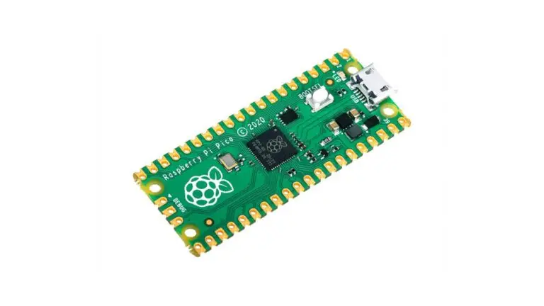
Dive into Raspberry Pi Pico projects! Explore hardware setups and creative ideas, from LED blinks to IoT wonders, perfect for makers and tech enthusiasts.

The ESP32-WROOM dev board is a versatile, dual-core IoT development platform with integrated Wi-Fi and Bluetooth, featuring 30+ GPIO pins for the wide range of peripherals. We’ll introduce its key

EMC basics: interference, test standards (FCC, CE), and PCB design fixes. Learn to pass EMC compliance with grounding/shielding. Essential for product certification!
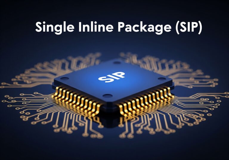
Understanding the Single Inline Package The single inline package (SIP) is a key player in electronic packaging. It offers a streamlined solution for integrated circuits. SIPs are known for their
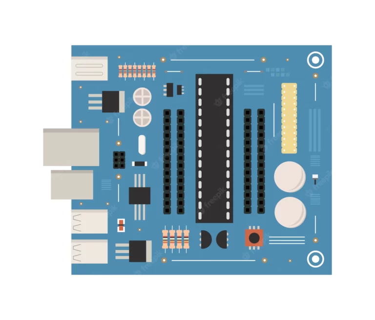
How many do you know about through hole vs surface mount? They are two ways to connect electronics components in pcb assembly (PCBA). They are cost-effective and reliable methods of

Interactive Guide to PCB Prototype Costs Goal: Inform/Engage -> Viz/Method: Interactive buttons -> Interaction: Click to reveal text -> Justification: Provides immediate, simplified value and engagement. – Report Info: Cost
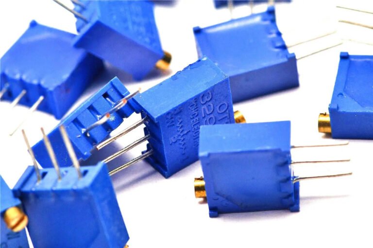
Potentiometers offer several advantages, including simple design, low cost, a wide resistance range, ease of operation, and mature technology. As reliable devices, they control, measure, and accurately sense voltage in
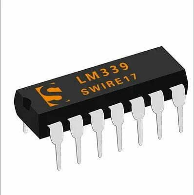
What is LM339 Comparator? LM339 is a common integrated circuit that contains four independent voltage comparators inside, making it a quad differential comparator. It is mainly used in high-voltage digital
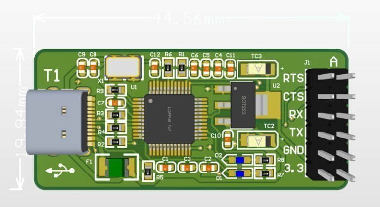
PCBs (printed circuit boards) and PCBA ( Printed Circuit Board Assembly) are both essential components of electronic devices. Both PCBs and PCBA refer to individual pieces within a larger system,
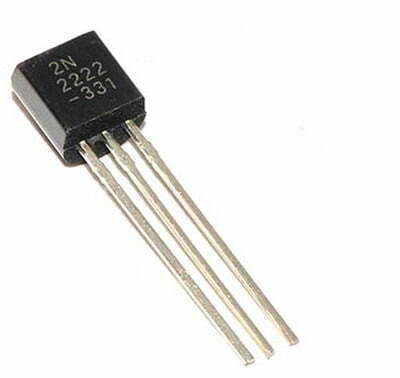
2N2222A NPN transistor specs: current gain, voltage limits, and switching applications. Learn to use in amplifiers and Arduino projects. Datasheet summary inside!

Debug embedded systems with JTAG, SWD, and logic analyzers. Learn setup, troubleshooting, and compatibility with STM32/Arduino. Essential guide for engineers!