What is Electromagnetic Compatibility?
Electromagnetic Compatibility (EMC) is the ability of an electrical device to function properly in its environment without being affected by electromagnetic interference from other devices, including those employing Ultra-Wideband (UWB) technology. Therefore, EMC includes two test standards: Electromagnetic Interference (EMI) and Electromagnetic Susceptibility (EMS). Read on to learn more about EMC and how you can prevent it from negatively affecting your electronics.
EMC Certification Standards
Electromagnetic compatibility standards are important for manufacturers who have to deal with EMC. There are many different emc standards and many different industries that need EMC testing.
International Organization
- IEC: The International Electrotechnical Commission, it includes 3 branches:
CISPR: International Special Committee on Radio Interference
TC77: Technical Committee on Electromagnetic Compatibility in Electrical Equipment (including Power Grids)
TC65: Industrial Process Measurement and Control
- ISO: International Organization for Standardization;
- IEEE;
- ETSI: the European Telecommunications Standards Committee;
- CCIR: International Radiocommunication Advisory Committee;
- ITU;
FCC: Federal Pass;
VDE: German Association of Electrical Engineers;
VCCI: Japanese civil interference;
BS: British Standard;
ABSI: American National Standard;
GOSTR: Russian government standard;
GB, GB/T: Chinese National Standard.
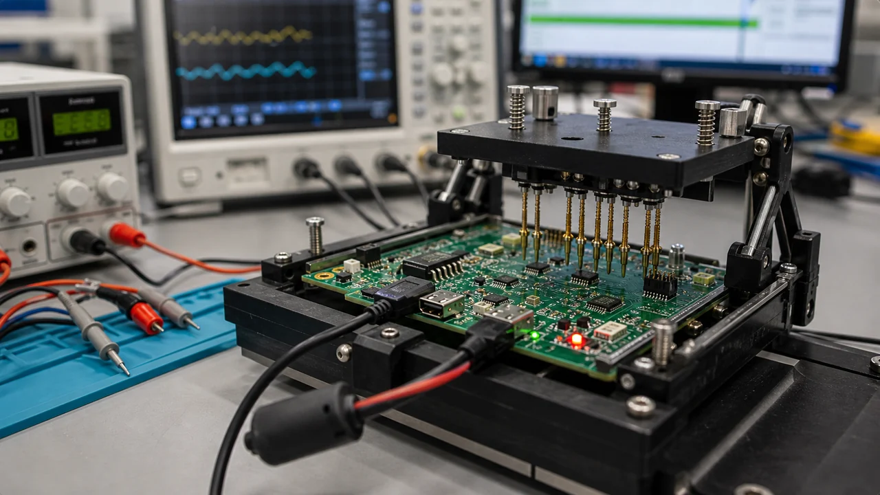
How to test electromagnetic compatibility?
There are many ways to test electromagnetic compatibility (EMC). One common method is to use an EMC chamber. This is a room that is specially designed to block out external electromagnetic fields, so that the only fields present are those generated by the device under test. By measuring the device’s response to various types of electromagnetic fields, it is possible to determine whether it is compatible with those fields. Other methods of testing EMC include using anechoic chambers and Faraday cages.
1. choose EMC testing laboratory
Shielded rooms, open areas, anechoic chambers, reverberation chambers, TEMs, and GTEMs are among the most common locations for EMC testing. Among them, anechoic chambers are the most common test locations. An anechoic chamber is used to shield electromagnetic waves other than the test equipment from interfering with other electromagnetic waves. Its principle is to absorb electromagnetic waves using ferrite absorbing materials to eliminate electromagnetic interference in the environment.
: Guide & Standards 1")
anechoic chambers
The currently known types of anechoic chambers can be divided into antenna pattern test rooms, radar cross section test rooms, electromagnetic compatibility (EMC) test rooms, and electronic warfare (countermeasures) test rooms according to their uses. The most common ones are full anechoic chamber and semi-anechoic chamber. The size and selection of RF absorbing materials are mainly determined by the layman’s size and test requirements of the equipment under test (EUT).
: Guide & Standards 2")
: Guide & Standards 3")
Test principle
The anechoic chamber is filled with cone-shaped absorbing materials, and there is a pyramid-shaped composite sponge absorbing body impregnated with absorbing powder. Its size is related to the absorbing frequency, and its function is also to absorb unnecessary electromagnetic waves and eliminate reflected signals. It can meet the electromagnetic wave absorption rate of 30MHz-40GHz frequency band and 10-20dB. The electromagnetic wave absorber used in the electromagnetic wave shielding anechoic chamber is adapted to the size of the anechoic chamber, and the thickness is continuously reduced in order to effectively utilize the space.
: Guide & Standards 4")
: Guide & Standards 5")
2. Select EMC test equipment
In the EMC test process, the supporting test equipment will be different according to the different industries of the equipment to be tested. details as follows:
EMI test equipment: EMI receivers, EMI accessories, conducted EMI test accessories, radiated EMI test antennas, harmonic flicker analyzers, near-field probes, etc.
EMS test equipment: EMS signal generator, EMS ancillary equipment, etc.
3. Test Procedure
Many different metrics can be used to measure EMC on an individual device or piece of equipment. However, there are a few metrics that are most common for EMC measurements for electronics.
EMI Testing metrics:
- Harmonic current (2nd to 40th harmonic);
- Flashing Flicker;
- Conducted disturbance (CE);
- Radiation disturbance (RE);
EMS Testing metrics:
- Electrostatic discharge immunity (ESD);
- Radiated electromagnetic field (80MHz~1000MHz) immunity (RS);
- Electrical fast transient/burst immunity;
- Surge (lightning strike) immunity;
- Injection current (150kHz~230MHz) immunity (CS);
- Voltage dip and short interruption immunity.
3.1 Harmonic Test
Harmonic testing mainly examines the influence of harmonics in low-voltage power supply networks on these frequency-sensitive equipment.
Test tandard: EN61000-3-2
- a) Specify limits for harmonic currents emitted to the public grid.
- b) Specify limits for the harmonic content of the input current generated by the equipment under test in the specified environment.
- c) Applicable to electrical and electronic equipment connected to the public low-voltage network with an input current less than or equal to 16A.
Principle of harmonic experiment: Due to the working mode of electronic equipment, nonlinear components and various interference noises, the input current is not a complete sine wave, and it often contains rich high-order harmonic components, causing pollution to the power grid. This phenomenon is called harmonic distortion.
3.2 Voltage Fluctuation and Flicker
The purpose of this standard is to ensure that the product does not cause undue flickering effects (flickering lights) to the lighting equipment it is connected to.
Test Standard: EN 61000-3-3
- a) Limits on the effects of constant voltage fluctuations and flicker on the public grid.
- b) Guidance for specifying limits and methods of evaluation of voltage variations produced by the prototype under test under specified conditions.
- c) It is suitable for 220V to 250V, 50Hz electrical and electronic equipment connected to the public low-voltage network with an input current of less than or equal to 16A per phase.
The picture below shows the allowable minute rate of change or change time for each relative voltage change value. It can be understood that the larger the voltage change range, the smaller the allowable change speed, or the longer the required change time.
: Guide & Standards 6")
Limits:
- Pst value should not be greater than 1.0;
- Pit value shall not be greater than 0.65;
- the value of d(t) during a voltage change shall not exceed 3.3% for more than 500ms;
- the relative steady-state voltage change, dc, shall not exceed 3.3%;
- maximum relative voltage change dmax shall not exceed 4%.
3.3 Conducted Emissions CE (0.15-30MHz)
Test Standard: EN61000-6-4
A) Electronic and electrical measurement and test equipment;
B) Electronic and electrical control equipment;
C) electrical and electronic laboratory equipment;
Classification of equipment
Class A: (non-household)equipment suitable for use in all establishments other than domestic and those directly connected to a low voltage power supply network which buildings supplies used for domestic purposes.
Class B: (Household)equipment suitable for use in domestic establishments and in establishments directly connected to a low voltage power supply network which supplies buildings used for domestic purposes.
experiment principle:
When the frequency of the interference noise of electronic equipment is less than 30MHz, it mainly interferes with the audio frequency band. For the wavelength of this type of electromagnetic wave, the cable of electronic equipment is less than the wavelength of one wave (the wavelength of 30MHz is 10m), and the radiation efficiency into the air is very low. In this way, if the noise voltage induced on the cable can be measured, the degree of electromagnetic noise interference in this frequency band can be measured, and this type of noise is conducted noise.
A line impedance stabilization network (LISN) is a device used to measure the electromagnetic interference (EMI) emitted by electronic devices. It is typically used in conjunction with an oscilloscope or spectrum analyzer.
: Guide & Standards 7")
The Effect of LISN:
1. Play a high-frequency isolation function between the EUT and the power supply to prevent noise from the power supply from entering the EUT, affect the measurement results.
2. Simulate the actual power supply impedance and provide a specified impedance between the power terminals of the EUT to unify the measurement results.
3. Keep the impedance in the test band stable at 50 ohms to achieve the input with the measurement receiver/spectrum analyzer impedance matching.
3.4 Radiated Emission RE (30-1000MHz)
Standard: EN61000-6-4
Classification of equipment
Class A: equipment suitable for use in all establishments other than domestic and those directly connected to a low voltage power supply network which supplies buildings used for domestic purposes. non-domestic
Class B: equipment suitable for use in domestic establishments and in establishments directly connected to a low voltage power supply network which supplies buildings used for domestic purposes.
a) Electrical and electronic measurement and test equipment
b) Electronic and electrical control equipment
c) Electrical and electronic laboratory equipment
The principle of radiated emission experiment:
When the total length of the antenna is greater than 1/20 of the signal wavelength λ, effective radiation emission will be generated into the space. When the length of the antenna is an integer multiple of λ/2, the radiated energy is the largest. When the noise frequency is greater than 30MHz, the cables, openings and gaps of electronic equipment are easy to meet the above conditions, resulting in radiation emission.
3.5 Electrostatic discharge (ESD)
The purpose of electrostatic discharge is to test the ability of a single device or system to resist electrostatic discharge interference.
Standard: IEC 61000-4-2 Criteria B
Experiment principle: The ESD experiment is to simulate the electrostatic discharge generated by the human body and objects when they contact the equipment, or the discharge of the human body and the object to the adjacent objects, including the direct exchange of energy, causing damage to the device or the near field (electric field and magnetic field) caused by the discharge. change), resulting in malfunction of the device.
3.6 radiated susceptibility (RS)
The purpose of radiated susceptibility is to test the ability of a single device or system to resist externally electric field disturbances.
Standard: IEC 61000-4-3 Criteria A
Test Waveform:
- Frequency range: 80MHz-2.5GHz
- Modulation: 80% AM, 1kHz sin-wave
- Frequency step size: 1%
- Dwell time: 3s
3.7 Fast Burst EFT
The purpose of the experiment is to investigate the ability of a single device or system to resist fast transient disturbances. These transient disturbances are caused by transient actions such as interruption of inductive loads, resulting in the appearance of pulse groups, high pulse repetition frequency, short rise time, and single pulse energy. Low level will cause the device to malfunction.
Standard: IEC 61000-4-4 Criteria B
3.8 Surge
The purpose of the experiment is to examine the ability of the EUT to resist surge interference. These transient disturbances are caused by short-circuit faults of other equipment, switching of the main power system, and indirect lightning strikes.
Standard: IEC 61000-4-5 Criteria B
3.9 Conducted Radio Frequency Interference (CS)
The purpose of the experiment is to examine the ability of a single device or system to resist conducted disturbances.
Standard: IEC 61000-4-6 Criteria A
Experimental principle: It mainly investigates the immunity of the continuous interference voltage of 0.15MHz-80MHz introduced from the wire or cable from the outside world, such as signals from an HDMI RF modulator.
Test Waveform:
- Frequency range: 0.15MHz-80MHz
- Modulation: 80% AM, 1kHz sin-wave
- Frequency step size: 1%
- Dwell time: 3s
3.10 Voltage dips
The purpose of the experiment is to investigate the ability of the EUT to resist voltage dips and sags.
Standard: IEC 61000-4-11 Criteria B & C
How to improve electromagnetic compatibility?
1. EMC shielding design
The effectiveness of your EMC shielding design relies on the type of material you choose as well as how it is implemented. You can further improve its performance by combining different types of materials together or by choosing a certain orientation for each specific layer of your shielding.
1.1 Ventilation hole and opening design
: Guide & Standards 8")
1.2 Structural lap joint shielding design
: Guide & Standards 9")
1.3 The cable passes through the shielding body
If the conductors pass out of the shield, the shielding effectiveness of the shield will be significantly degraded. This penetration is typically when the cable exits the shield.
: Guide & Standards 10")
1.4 Design principles for cables going out of the shielding body
1.4.1 When shielded cables are used, when the shielded cables exit the shielding body, the clip wire structure is adopted to ensure reliable grounding between the shielding layer of the cable and the shielding body and provide a sufficiently low contact impedance.
1.4.2 When using shielded cables, use shielded connectors to transfer the signals out of the shielding body, and ensure the reliable grounding of the shielding layers of the cables through the connectors.
1.4.3 When using an unshielded cable, use a filter connector to transfer. Due to the high frequency characteristic of the filter, it is ensured that there is a sufficiently low high frequency impedance between the cable and the shield.
1.4.4 When using unshielded cables, the cables should be short enough inside (or outside) of the shield to prevent interference signals from being effectively coupled out, thereby reducing the impact of cable penetration.
1.4.5 The power line goes out of the shield through the power filter. Due to the high-frequency characteristic of the filter, it is ensured that there is a sufficiently low high-frequency impedance between the power line and the shield.
1.4.6 Using optical fiber outlet. Since the optical fiber itself has no metal body, there is no problem of cable penetration.
1.5 Poor grounding
: Guide & Standards 11")
1.6 Shielding materials and applications
The materials we use for shielding include conductive cloth, reed, conductive rubber, and specialized PCB coatings.
: Guide & Standards 12")
1.7 Cut-off waveguide ventilation plate
: Guide & Standards 13")
2. EMC grounding design
2.1 The concept and purpose of grounding
2.1.1 One is for safety, called protective grounding. The metal casing of electronic equipment must be connected to the ground, so as to avoid the occurrence of excessive ground voltage on the metal casing due to accidents, which may endanger the safety of operators and equipment.
2.1.2 The second is to provide a low-impedance path for the current to return to its source, that is, the working ground.
2.1.3 Lightning protection grounding to provide current discharge for lightning strikes.
2.2 Grounding provides signal return
: Guide & Standards 14")
2.3 Single point grounding
Suitable for systems with operating frequency below 1MHz.
: Guide & Standards 15")
2.4 Multi-point grounding and mixed grounding
: Guide & Standards 16")
3. EMC Wave filter design
3.1 Wave Filter Definition
A wave filter is a device that alters the frequency content of a signal by selectively attenuating certain frequencies while allowing others to pass.
: Guide & Standards 17")
3.2 Type of wave filters
The common filter types include: low pass filter, high pass filter, band-pass filter, and band-stop filter. As figure shows below:
: Guide & Standards 18")
If a filter passes low frequencies and blocks high frequencies, it is called a low pass filter. If it blocks low frequencies and passes high frequencies, it’s a high pass filter. There are also bandpass filters, which pass only a relatively narrow frequency range. And a band-stop filter, which blocks only a relatively narrow range of frequencies.
3.3 Wave Filter components
3.3.1 Capacitor (general capacitor, three-terminal capacitor);
3.3.2 Inductance (general inductance, common mode inductance, magnetic beads);
3.3.3 Resistance;
3.4 Differential mode filter and common mode filter design
: Guide & Standards 19")
4. EMC PCB Design
4.1 PCB design
4.1.1 Layout: similar circuits are arranged in one piece, the principle of controlling the minimum path, high-speed circuits should not be close to the small panel, and the power module should be close to the position of the single disk.
4.1.2 Layering: The high-speed wiring layer must be close to a ground layer, the power supply is adjacent to the ground, a layer of ground should be placed under the component surface, two surface layers may be placed close to the ground layer, and the inner layer should be indented by 20H compared to the surface layer.
4.1.3 Wiring: Short traces, optimal trace width and wide spacing between different types of traces (except for signals and their return lines, differential lines, and shielded ground lines), fewer vias, no loops, small loop area, wireless head.
4.1.4 Grounding: similar circuits are distributed separately and connected at a single point on the board.
4.1.5 Filtering: power supply module, functional circuit design board-level wave filter circuit.
4.1.6 Interface circuit design: interface circuit design filter circuit to achieve effective isolation between inside and outside.
4.2 The basic principles of layout
4.2.1 Referring to the functional block diagram of the principle, based on the signal flow, it is divided into functional modules.
4.2.2 Separate layout of digital circuits and analog circuits, high-speed circuits and low-speed circuits, interference sources and sensitive circuits.
4.2.3 Avoid placing sensitive devices or strong radiation devices on the welding surface of the single board.
4.2.4 The loop area of sensitive signals and strong radiation signals is the smallest.
4.2.5 Strong radiation devices or sensitive devices such as crystals, crystal oscillators, relays, switching power supplies, etc. should be placed away from single-board handle bars, external interface connectors, and sensitive devices. The recommended distance is ≥1000mil.
4.2.6 Sensitive devices: keep away from strong radiation devices, the recommended distance is ≥1000mil.
4.2.7 Isolation devices, A/D devices: the input and output are separated from each other, and there is no coupling path (such as adjacent reference planes), preferably across the corresponding partition.
4.3 Special device layout
4.3.1 Power part (placed at the power inlet).
4.3.2 Clock part (away from the opening, close to the load, wiring inner layer).
4.3.3 Inductive coil (away from EMI source).
4.3.4 Bus driver part (inner layer of wiring, away from the opening, close to the sink).
4.3.5 Filter components (separate input and output, close to the source, short leads).
4.4 Layout of filter capacitors
4.4.1 All branch power supply interface circuits.
4.4.2 Near components with high power consumption.
4.4.3 Areas with large current changes, such as input and output terminals of power modules, fans, relays, etc.
4.4.4 PCB power interface circuit.
4.5 Layout of decoupling capacitors
4.5.1 close to the power pins.
4.5.2 Appropriate location and quantity.
4.6 The basic principles of the layout of the interface circuit
Devices such as filtering, protection, and isolation of interface signals are placed close to the interface connector, and they are protected first and then filtered.
Isolation devices such as interface transformers and optocouplers are completely isolated from the primary and secondary.
No crossover of signal network between transformer and connector.
The BOTTOM layer area corresponding to the transformer should be placed as far as possible without other devices.
The interface chip (network port, E1/T1 port, serial port, etc.) should be placed as close as possible to the transformer or connector.
4.7 Wiring
Short traces, wide spacing between different types of traces (except for signals and their return lines, differential lines, and shielded ground lines), fewer vias, no loops, small loop area, wireless head.
For traces with delay requirements, their lengths meet the requirements.
There is no right angle, and arc chamfering is preferred for key signal lines.
The signal traces of adjacent layers are perpendicular to each other or the parallel wiring of key signals of adjacent layers is less than or equal to 1000MIL.
PCB Design and Manufacturing Notes for EMC (Electromagnetic Compatibility): Guide & Standards
These additions address practical search intent while preserving the original page structure and existing ranking content.
- Define stack-up, laminate, copper weight, minimum trace/space, annular ring, solder mask, and IPC class before releasing fabrication files.
- Run DRC/DFM checks against the chosen manufacturer’s capability table, especially for impedance control, via aspect ratio, solder mask slivers, and drill tolerances.
- Include fiducials, tooling holes, panelization notes, test coupons, and controlled-impedance requirements when the board moves beyond prototype quantity.