What is a through-hole PCB?
The through hole is a hole in an electrically conductive material (such as an printed circuit board (PCB)) through which leads are soldered, that is plated with a metal. The metal is occasionally chosen to be more corrosion-resistant than the solder, while being electrically more conductive than solder. Materials used include brass, copper and stainless steel.
Where are through-hole PCBs used?
Instead of making a surface mount version of a PCB, manufacturers can use through-hole components for certain applications, where it makes sense to have holes instead of pads.
A through-hole PCB has mounting holes on one side that are large enough for a standard drill bit or other tools for fastening components with screws or bolts. The other side of the board often has copper pads so that components can easily be soldered to the back side of the board.
types of holes in pcb
Through-hole printed circuit board (TH PCB or TH board) is the most common type of printed circuit board used in electronics. Through-hole boards can be further broken down into single-end and double-end versions. Traditionally, it is divided into 3 types on pcb:
- Plated Through Hole(PTH)
A plated-through hole is a type of through hole (a hole passing all the way through a printed circuit board) that is plated on both sides with a metal layer, typically copper.

- Buried Via Hole(BVH)
A buried via hole is a via hole that has been plated over with copper, making it invisible. In many circuit boards, there are copper plated areas which are designed for wire-wrapping connections. These copper plated areas can become oxidized or damaged. Buried vias provide a way to repair or replace these connections. A buried via may be visible if a damaged wire is replaced or if repair work is done on the board.
- Blind Via Hole(BVH)
A blind via is a copper plated hole that connects the top or bottom layer of the printed circuit board to one or more of the inner layers.
Advantages of a Through-Hole PCB
- Longer Lifespan
Through-hole components can last for decades, while surface-mount components only last for a few years. This is because more of the component is exposed to the environment and can corrode, while surface-mounted components only have contacts on the surface.
- Easier to Find Replacement Parts.
Unless your product is still in production and uses surface-mount technology (SMT) circuit board, you’ll be able to find replacement parts for through-hole designs.
- Lower Cost
Through-hole boards are cheaper to produce and assemble. To assemble an SMT product, workers must use expensive pick-and-place robots to put the components in the right place, which is expensive.
- Easier to Mount Wires
You can easily wrap wires around a through-hole board to secure them instead of using special adhesives and hot-melt glue that are used with surface-mount boards.
Disadvantages of a Through-Hole PCB
- Longer Time to Assemble
Through-hole boards take longer to assemble than SMT boards because a special pneumatic or mechanical press is needed to assemble the boards, and workers must use a soldering iron to complete the job.
- Risk of Mistakes
The handling of through-hole boards is more manual, so there is a greater risk of mistakes during the assembly process
- Heavier Weight
Through-hole boards have more components and larger components than SMT boards, which makes them heavier.
how are through-hole PCBs made?
1. Create Schematic Diagram
The first step in the process is to create a computer-aided design (CAD) schematic.

2. PCB Layout
A layout diagram is a visual representation of the electrical and physical routing of components and their interconnections. This is where you input all the data, such as the dimensions, materials, traces and so on.


Tip
It may also include annotations such as a description of the materials used, any special mounting requirements, or a note on the type of construction used.
3. PCB Photoresist & Image transfer
3.1 PCB Photoresist
The next step is to create a photoresist PCB layout used to create the PCB assembly image.

To do this, you place the layout diagram in a photo-mask machine that projects a pattern of light onto the layout diagram. The light pattern goes through the diagram onto a thin sheet of chemically treated paper (called photoresist). Once the photoresist is exposed, it is developed with a solvent.
3.2 PCB Image Transfer
In general, pcb inner layer image transfer is not necessary because PCB inner layer usually is not exposed to the outside environment. However, if you want to make your product more beautiful or if you want to protect your product from damage, pcb inner layer image transfer is recommended.

4. PCB Inner Layer Etching
A PCB inner layer etching is a process of removing the copper(I) on the layer below the copper foil, which is immersed in an acid solution.
The reason for this is that the copper on the surface of the PCB may act as an insulator and prevent good connection with the electrolytic or solid polymeric parts.

In order to remove this layer, one may use an etching solution (such as sulfuric acid, nitric acid or concentrated sulfuric acid). The solution can be poured into a tank and immersed into it a PCB (with the copper on its surface). When the solution reaches its active phase, we may remove the PCB from it.
Tip
While etching PCB inner layer, remember that flux transfer is not possible and you have to take care of transferring it in right direction.
5. inner dry film stripping
The pcb inner dry film stripping involves the stripping of the film coating from the PCB (Printed Circuit Board) allowing the individual components on the surface of the PCB to be visible through a transparent layer.
The pcb inner dry film stripping can be done manually by using a scraper and/or manually ejecting the coating with a device like a DesoxIT, or automatically with a device like a DRI-RAD or DRI-RAS.

Tips
a) pcb inner dry film stripping is a cost effective and risk free way to clean and scrap pcb’s without damaging pcb surface.
b) It involves immersion of pcb in a solvent bath for some time to get rid of the coating on pcb surface.
c) It can be used on pcb’s with no PCB markings on it and also on pcb’s with markings like EMI shielding, RF shielding etc.
6. PCB Through-holes drilling
The next step is to drill the panel to create holes for mounting the components on the PCB. The panel is placed underneath a drilling machine, which uses tools such as rotary bores and PTH drill to create through-holes in pcb substrates.

7. PCB copper cladding
Then, coat the exposed copper panel with a thin layer of copper. You can do this by electroplating or electroless plating.

8. solder mask
The PCB solder mask is the coating that is placed on the PCB to reduce the amount of scale that forms on the boards surface as a result of exposure to moisture. The solder mask is made of a resin that adheres to the boards surface, and has a dielectric coating on both sides.

9. External layer photoresist
PCB External Layer Photoresist is used to create freestanding photoresist structures on a PCB in a manner similar to flexographic printing.
The photoresist is applied to the PCB using a spin coater or an oscillating belt coater and cured either in UV or visible light, following any specific process provided by the manufacturer. The resultant freestanding photoresist structures can then be mated with the circuitry pattern prior to etching.

10. External layer image transfer
For external layer transfer, it is possible to achieve by using wet wipe and paper transfer. Transfer wet wipe and paper on insulator material like PET or PE lamination.

When using ENIG process for PCB manufacture it is necessary to follow the below process:
1). Immersion in nickel bath.
2). Area drying/Desensitization.
3). Washing with Agua.
4). Washing with aqua dip.
5). Second immersion into bath.
6). Final drying /curing unit.

12. Electro-tinning
electro-tinning is a process where a high-density polyethylene (P.H.D.P) film is electroplated onto the surface of a printed circuit board (PCB).
The PCBs are first coated withsilane to act as an anode and the electrolyte as a cathode, and then plated by applyinga low voltage between the electrical contacts on the PCB and the electrolyte.

13. Outer Wet film stripping
Outer wet film stripping is performed between the board and surrounding plastic or metal housing components, to remove paint or plating from circuit boards before assembly into finished products.

14. Outer Layer etching
The pcb outer layer is etched to produce the following parts:
a) An opening for wires to pass through for soldering.
b) A defining pattern on the pcb for routing.
c) An opening for components to be soldered onto the pcb.
d) A plating of the pcb surface that allow it to be bonded against a printed circuit board.

Tip
While etching PCB outer, conductive layers, it is important to protect PCBs from oxides and particles in air, because they may get into chips and can cause short circuit or destroy chip. Therefore before etching PCB outer layer, you should collect all the dust and dispose them in a safe way.
15. Tin stripping
Tin stripping is the process of removing the tin and copper from PCB. It can be done in a number of ways, depending on the type of product, the availability of materials and the skills and experience of the operator.
a). The most common way to strip PCB tin is by using solvent. Solvent-based stripping is effective, but time consuming and can result in the formation of toxic byproducts.
b). Another option is to use acid or hydrochloric acid. Acid-based stripping is faster, but results in lower quality tin.
c). A third option is to combine the two methods, using solvent to remove the paint followed by acid to strip the remaining tin.

Hasl is a soldering process that removes the excess solder from a printed circuit board (PCB).
The process of HASL is simple: the excess solder is burned off of the PCB by heating the board above its melting point with a hot air gun.

Tip
While this method works fine, it has limitations:
a). The hot air gun can only be used for a few seconds at a time.
b). Additionally, due to surface imperfections on PCBs, some solder will inevitably break away from the board and remain on the gun itself.
c). No flat surface available for your board, so you have to cope with it.
d). You need two pieces of board for hold each other.
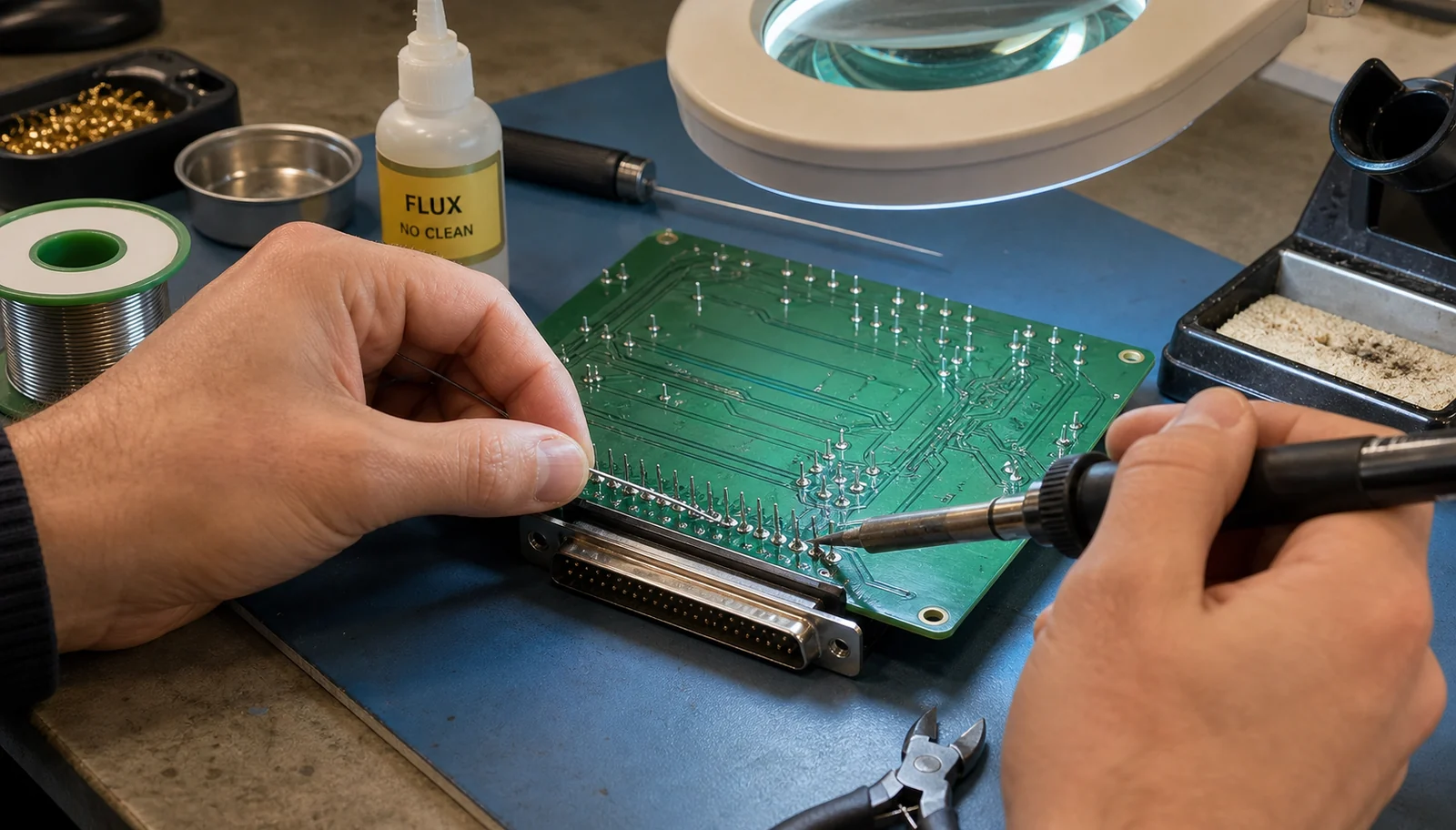
17. through hole PCB assembly
There’re several ways on through hole pcb assembly:
- Place the components
Surface mount technology (SMT) is most efficient option for assembling large mount of through- hole PCB. SMT allows for components to be mounted directly on top of the board using pins, which connect to pads on the board surface.


- through hole PCB soldering
After the components are placed on the pcb, you can solder them together with pick-and-place equipment. You can also make connections between the components using wires, conductive adhesives, or other components to form an electrical circuit.

pcb soldering tips:
9 Essential Electronics Soldering Tips and Tricks for Beginners
18. through hole PCB test
Once the assembly process is completed, it’s tested to make sure all the components are working as they should.

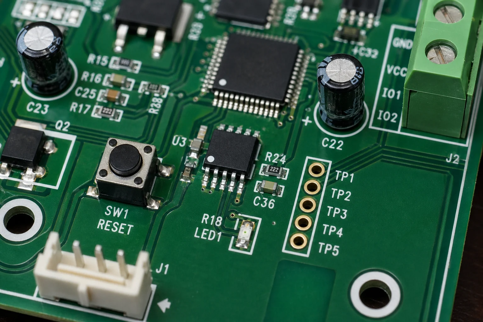
T-Hole test point
Hole test point is a discreet hole in the printed circuit board that allows you to access the internal signals (pins) of a component, or to connect wires or jumpers to these pins.
In addition, they can also be used to connect signals between two different components without modifying the circuit board.
Through Hole PCB Size
There is no official standard for through-hole pcb size. However, here are some guidelines that can be followed to get good results:
1. The type of component that the PCB is going to be used for.
2. The characteristic of the component (size, shape and weight).
3. The material the component is made out of.
4. The quantity and the size of the component in question.
5. The capacity of the PCB hole machine that is being used to produce the hole size on PCB (if any).
PCB Through Hole Size Chart

Tips
The smaller the hole, the less lead traces will be needed;
The smaller the hole, the higher signal loss;
The smaller the hole, the more difficult it is to drill accurately.
pcb through hole size calculator
The Saturn PCB Toolkit is a great freeware resource for PCB calculations, particularly for designers and engineers. It includes numerous useful features, such as the via hole diameter, current capacity of a circuit track, current, differential pairs, and more.