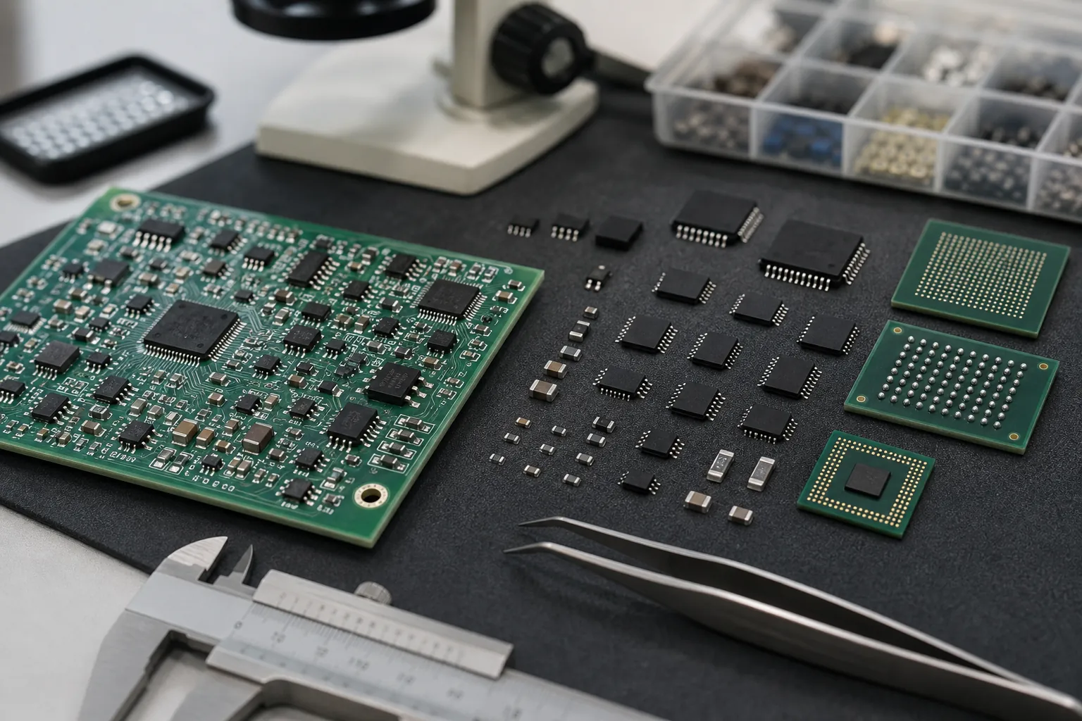
4 Layer PCB is a vital part of the electronic components that make up modern devices. Every single electronic component has an electronic counterpart somewhere on the PCB, and in turn, every PCB has holes to hold these electronic components. But what is the difference between 4-layer, 6-layer, 8-layer and 10-layer PCBs? And why do some manufacturers recommend certain thicknesses over others? Let’s take a look.
how many layers PCB can have?
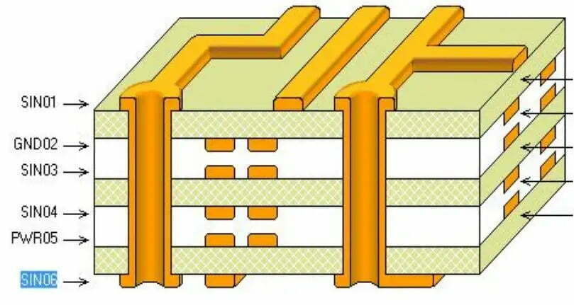
PCB has many layers and each one of these layers is an essential part of your finished PCB. There are some commonly known layers like top, bottom, substrate and so on, but there are more layers also. These additional layers are referred as “functional layers”. Some of the commonly used functional layers are shown below.
- Copper Revision layer:
This is the first layer that gets deposited on the PCB. This is a critical layer as it decides how the rest of the layers are going to be deposited. It decides how the rest of the layers are going to be deposited. - Solder mask layer:
This is a thin layer that protects the topmost layer from oxidization. For more details on protecting PCBs, see our article on PCB coating. - Top solder mask:
This is a thicker layer of copper that protects the topmost layer from oxidization. - Bottom solder mask:
This is a thicker layer of copper that protects the bottommost layer from oxidization. - Substrate:
This is the base material of the PCB and it has to be hard enough for the PCB to be attached to. - Dry film:
This is a coating of resin that is applied over the substrate. - Wet film:
This is the completion of the PCB process and the print head moves over to deposit the copper. - Adhesive layer:
This is a thin copper layer that is applied over the wet film to complete the PCB process.
4 Layer PCB
A 4-layer PCB is the base layer of your printed circuit board (PCB). The base layer is where the traces are laid down to transfer signals between the components. The base layer is made of polyimide or polyester. Polyimide is commonly used in military PCBs as it has a very high dielectric strength and is resistant to chemicals, oil and grease. Polyester is commonly used in consumer-grade PCBs as it is highly flexible and can be easily processed with low tension.

4 layer PCB stackup
There are 2 types of stackup for 4 layer pcb board:
Stackup 1
– Layer 1: Signal
– Layer 2: Ground/Power
– Layer 3: Power/Ground
– Layer 4: Signal
Stackup 2
– Layer 1: Ground
– Layer 2: Signal/Power
– Layer 3: Power/Signal
– Layer 4: Ground
For the first stackup, it is usually applied to the situation where there are many chips on the board. This solution can get better SI performance, but it is not very good for EMI performance, which is mainly controlled by wiring and other details. Main attention: The formation is placed on the connecting layer of the signal layer with the most dense signal, which is conducive to absorbing and suppressing radiation; increasing the board area to reflect the 20H rule.
The second approach is used when the board has enough space around the chip and the chip density is low enough. The outer layers of the PCB function as ground lines, and the middle layers function as signal/power lines. The power supply is routed on the signal line using a wide wire, making the impedance of the power supply current low and the impedance of the signal microstrip path low. This structure also has the lowest EMI performance of any 4-layer PCB.
4 Layer PCB Advantages
- – More routing options than two layer boards;
- – Can handle higher currents than two layer boards;
- – Less likely to be damaged by electrostatic discharge.
4 layer PCB Applications
Four layer PCBs are used in a variety of applications, including:
- – automotive electronics;
- – telecommunications;
- – computer networking;
- – medical devices;
- – aerospace and defense.
6 layer PCB
Next up, we have a 6-layer PCB. Like the 4-layer PCB, the 6-layer PCB is also made of polyimide or polyester. However, in this case, the thickness of each of these layers is increased. This increases the rigidity of the PCB and makes it more durable.
6 Layer PCB Stackup
In order to handle the high instantaneous bandwidth and the massive number of chips, you should use a 6-layer board. The following stacking configuration is recommended:
Stackup 1
– Layer 1: Signal
– Layer 2: Ground
– Layer 3: Signal
– Layer 4: Power
– Layer 5: Ground
– Layer 6: Signal
Stackup 2
– Layer 1: Ground
– Layer 2: Signal
– Layer 3: Ground
– Layer 4: Power
– Layer 5: Signal
– Layer 6: Ground
For Stackup 1, the signal layer is adjacent to the ground layer and the ground and power layers are paired, resulting in better signal integrity. The impedance of each trace layer can be well controlled, and the two layers are able to absorb magnetic field lines well. When the complete power and ground layers are present, the return path for each signal layer is improved.
For Stackup 2, this solution is only suitable for the case where the device density is not very high. This stack has all the advantages of the stack above, and the ground plane of the top and bottom layers is relatively complete and can be used as a better shielding layer to use. It should be noted that the power layer should be close to the layer that is not the main component side, because the bottom plane will be more complete. Therefore, its EMI performance is better than the first scheme.
6 Layer PCB Advantages
- – Better mechanical stability and heat dissipation;
- – Increased routing density;
- – Higher current and voltage carrying capacity;
- – Improved reliability;
- – Reduced crosstalk;
- – Reduced electromagnetic interference.
6 layer PCB Applications
- – High-speed digital and RF applications;
- – Power amplifiers;
- – Microwave devices;
- – High-voltage/high-current applications;
- – Impedance-controlled transmission lines;
- – EMI/RFI shielding.
8 layer PCB
The 8-layer PCB is the thickest of all PCBs and is made of polyimide or polyester. Polyimide PCBs are extremely durable and flexible while also being able to process through automated systems relatively easily. Polyester PCBs are extremely flexible but are unable to withstand chemical resistance like polyimide PCBs. They can be more expensive to manufacture than lower layer counts. And they require more careful design and planning.
8 Layer PCB stackup
There are many possible ways to stack up an 8 layer PCB, but here is the best one example:
– Layer 1: Signal
– Layer 2: Ground
– Layer 3: Signal
– Layer 4: Power
– Layer 5: Ground
– Layer 6: Signal
– Layer 7: Ground
– Layer 8: Signal
The inner layers are typically used for carrying signals, while the outer layers are used for providing power or ground planes. This stacking method helps to reduce crosstalk and improve signal integrity. Further more, it has a very good ability to absorb geomagnetism, since the use of multiple layers of ground.
8 layer PCB Advantages
- – Reduced Crosstalk;
- – Reduced Electromagnetic Interference;
- – Reduced Signal Loss;
- – Increased Signal Integrity;
- – The eight-layer PCB offers more routing capabilities than the four-layer PCB;
- – An eight-layer PCB can support a higher component density.
8 layer PCB Applications
8 layer PCBs are often used in high-speed or complex designs, some common use include:
- – Power supply boards;
- – Communication boards;
- – Control boards;
- – Signal boards;
- – Memory boards;
- – Interface boards;
- – Data acquisition boards;
- – Embedded systems boards.
Engineering checks for What is the difference between 4-layer, 6-layer, 8-layer PCBs?
Before using What is the difference between 4-layer, 6-layer, 8-layer PCBs? in a PCB, firmware, repair, or validation workflow, confirm the details that usually decide whether the design works reliably instead of only reading the headline specification.
Design and troubleshooting checklist
| Area | What to check | Why it matters |
|---|---|---|
| Design data | Connect 6 layer vs 8 layer pcb to the schematic, BOM, stackup, footprints, and manufacturing notes | PCB decisions must stay traceable to source data |
| Manufacturing | Check clearances, solderability, thermal relief, silkscreen, test pads, and IPC requirements | Manufacturing rules prevent rework and field failures |
| Inspection | Validate with DRC, visual inspection, continuity, functional test, and failure analysis | Testing closes the loop between design and production |
These checks help connect the search intent around 6 layer vs 8 layer pcb with practical board-level decisions, component selection, and failure analysis.