In recent years, the redistribution layer (RDL) technology has gained significant traction. It’s a revolutionary packaging solution that has transformed the way we package ICs.
In this article, we’ll explore the definition of RDL, its function, benefits, process, application, and comparision with other IC packaging technologies.
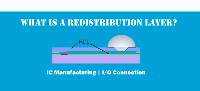
What is Redistribution Layer Technology?
Redistribution layer, also known as RDL, is a layer of metal that is added to an integrated circuit or microchip to redistribute the electrical connections. This RDL technology is an advance packaging solution for integrated circuits (ICs), which allows the integration of multiple dies into a single package. It is a process of creating a patterned metal layer on top of the dielectric layer, which redistributes the input/output (I/O) of the IC to a new location. The new location is typically at the edge of the die, which allows the IC to be connected to the printed circuit board (PCB) using standard surface mount technology (SMT). The RDL technology enables the designer to place the die in a compact and efficient way, thereby reducing the overall footprint of the device.
 Technology for ICs Package 1")
The RDL technology is crucial in the development of modern electronic devices that are becoming increasingly compact and complex. It enables chips to be smaller, faster, and more efficient. It is usually used in the packaging of MEMS devices, sensors, power devices, memory, microprocessors, and graphic processors.
Function of Redistribution Layer
The redistribution layer (RDL) plays a critical role in extending and interconnecting the XY plane in chip design and manufacturing.
 Technology for ICs Package 2")
Redistribute the I/O Connection
I/O (input/output) pads are chip pin processing modules usually distributed on the edge or periphery of the chip. They can process the signal of chip pins and output the signal of the chip to the pin after processing.
RDL can facilitate the redistribution of the I/O connections from the chip to the package. The RDL connects the bond pads on the chip to the package leads or balls, which allows for easier assembly and better performance of the IC.
This is naturally convenient for the bond wire process but is somewhat challenging for flip chips. Therefore, RDL became the key to this moment. It deposits a metal layer and corresponding dielectric layer on the surface of the chip, forming a metal wire and redesigning the IO ports to a new, more spacious area, forming a surface array layout.
Route Signals and Power
In addition, the RDL also provides a means to route signals and power within the IC. The use of RDLs has become increasingly important as ICs have become more complex and require more I/O connections. They are used in a wide range of applications, such as microprocessors, memory chips, and sensors.
Benefits of Redistribution Layer
The RDL technology offers several benefits for designers who are looking to create high-performance, compact, and cost-effective electronic devices. Some of the benefits of using RDL technology in ICs package are:
Reduced Footprint
The RDL technology allows the integration of multiple dies into a single package, thereby reducing the overall footprint of the device. This enables designers to create smaller and more compact electronic devices, which is essential for applications such as smartphones, wearables, and IoT devices.
Improved Electrical Performance
The RDL technology enables the designer to place the die in a compact and efficient way, which reduces the length of the interconnects. This, in turn, reduces the signal delay and improves the electrical performance of the device. The RDL technology also reduces the parasitic capacitance and inductance, which improves the signal integrity of the device.
Reduced Cost
The RDL technology eliminates the need for wire bonding and flip-chip bonding, which are expensive and time-consuming processes. The RDL technology also reduces the number of components required for the device, which further reduces the cost of the device. The RDL technology is a cost-effective solution for creating high-performance ICs that require a small form factor.
Types of Redistribution Layer Technology
There are two types of redistribution layer (RDL) technology: fan-in and fan-out. The fan-in RDL technology is used for packaging a single die, whereas the fan-out RDL technology is used for packaging multiple dies.
Fan-in RDL Technology
The fan-in RDL technology is used for packaging a single die. The fan-in RDL technology is also known as wafer-level package (WLP), which is a process of creating a package directly on the wafer. The fan-in RDL technology is a cost-effective solution for creating small and thin packages.
The fan-in RDL technology is suitable for applications such as sensors, MEMS devices, RF devices, microprocessors and memory devices.
Fan-out RDL Technology
The fan-out RDL technology is used for packaging multiple dies. The fan-out RDL technology is also known as wafer-level fan-out (WLFO), which is a process of creating a package on a reconstituted wafer. The fan-out RDL technology is a cost-effective solution for creating high-performance packages with a small form factor.
The fan-out RDL technology is suitable for applications such as graphic processors, system-on-chip (SoC), memory devices, power devices and LED devices.
Redistribution Layer Process
The RDL technology is a complex process that involves many steps such as dielectric deposition, metal deposition, patterning, and etching. Below are the process flow for Fan-in RDL and Fan-out RDL.
Fan-in RDL Process
The Fan-in RDL process is used in the production of advanced packaging solutions such as Wafer-Level Chip-Scale Packaging (WLCSP) and System-in-Package (SiP) designs. It allows for higher levels of integration, reduced form factors, and improved performance for semiconductor devices. The process involves multiple steps as below:
 Technology for ICs Package 3")
The process starts with an incoming wafer, which is then coated with PI (Photoresist Insulator) in step 1. This is followed by PI exposure in step 2, PI development in step 3, and PI cure in step 4.
In step 5, a seed layer is sputtered onto the wafer, which is then coated with resist in step 6. The resist is then exposed in step 7, developed in step 8, and the RDL is plated in step 9.
After that, the resist is stripped off in step 10, and a dry film is laminated onto the wafer in step 11. The dry film is then exposed in step 12 and developed in step 13. Next, copper posts are plated onto the wafer in step 14, and the dry film is stripped in step 15.
In step 16, the seed layer is etched, and in step 17, a front side mold is created. The mold is then cured in step 18, and the wafer is mechanically buffed in step 19. Finally, in step 20, the excess copper is etched back, completing the Fan-in RDL process flow.
Fan-out RDL Process
Similar to the Fan-in RDL process, the Fan-out RDL process is also a way to create smaller, higher-performing chip packages with more connections. Here are the manufacturing steps:
 Technology for ICs Package 4")
1. Wafer probe: This is the initial testing of the wafer to ensure that it meets the required specifications before moving on to the subsequent processing steps.
2. Wafer backgrind: The backside of the wafer is ground down to a specified thickness to reduce the thickness of the package.
3. Wafer saw: The wafer is cut into individual dies.
4. KGD (Known Good Die) pick and place: The good dies are picked up and transferred onto a carrier wafer with adhesive.
5a. Wafer mold: The wafer with the dies attached to the carrier wafer is molded with a dielectric material to form a fan-out structure.
5b. Carrier and temporary adhesive removal: The carrier wafer is removed from the fan-out wafer, and any temporary adhesive used during the process is also removed.
5c. Fan-out wafer clean: The fan-out wafer is cleaned to remove any remaining particles or impurities.
6. Polymer 1 coat: A polymer layer is applied to the surface of the fan-out wafer to act as a dielectric layer.
7. Polymer 1 image/develop/cure: The polymer layer is patterned using photolithography to create the desired shape and size of the RDL structure.
8. RDL seed layer sputter: A thin layer of copper or other conductive material is deposited on top of the polymer layer using sputtering.
9. Resist coat: A layer of resist material is applied over the seed layer.
10. Resist image/develop: The resist layer is patterned using photolithography to create the desired shape and size of the RDL structure.
11. RDL copper pattern plate: Copper is deposited on top of the exposed areas of the seed layer using electroplating, creating the desired RDL pattern.
12. Resist strip: The remaining resist material is removed, leaving only the copper RDL pattern.
13. Seed layer etch: The unneeded portion of the seed layer is removed using etching.
14. Polymer 2 coat: Another polymer layer is applied on top of the RDL structure to act as a dielectric layer.
15. Polymer 2 image/develop/cure: The polymer layer is patterned using photolithography to create the desired shape and size of the UBM structure.
16. UBM seed layer sputter: A thin layer of copper or other conductive material is deposited on top of the polymer layer using sputtering.
17. Resist coat: A layer of resist material is applied over the seed layer.
18. Resist image/develop: The resist layer is patterned using photolithography to create the desired shape and size of the UBM structure.
19. UBM pattern plate: Copper is deposited on top of the exposed areas of the seed layer using electroplating, creating the desired UBM pattern.
20. Resist strip: The remaining resist material is removed, leaving only the copper UBM pattern.
21. Seed layer etch: The unneeded portion of the seed layer is removed using etching.
22. Flux print: A flux material is applied to the UBM pads.
23. Solder ball drop: Solder balls are placed onto the UBM pads.
24. Solder reflow: The solder balls are heated to melt and form connections between the UBM pads and external leads or bumps.
25. Fan-out wafer probe: The packaged IC is tested to ensure that it meets the required specifications.
26. Laser mark: A unique identifier or barcode is etched onto the surface of the IC using a laser.
27. Wafer saw: The fan-out wafer is cut into individual packages.
28. Tape and reel: The individual packaged ICs are mounted on a reel for easy handling and shipping.
Apply RDL to Advanced Packaging
In advanced packaging such as fan-in wafer-level package (FIWLP) and fan-out wafer-level package (FOWLP), RDL is the most critical technology. It is the rise of this technology that has enabled packaging plants to compete with wafer foundries in fan-out packaging technology. Through RDL, IOPad can be made into different types of wafer-level packages in FIWLP or FOWLP. In FIWLP, bumps are all grown on the die, and the connection between the die and the pad mainly depends on the metal line of RDL. After packaging, the IC is almost the same size as the die area. In FOWLP, bumps can grow outside the die, and the IC after packaging is larger than the die area (1.2 times).
In particular, in 2.5D advanced packaging, besides the TSV on the silicon substrate, RDL is also indispensable. Taking TSMC’s InFO, a representative of 2.5D advanced packaging, as an example, InFO uses one or more bare dies on the carrier, which are then embedded in the reconstituted wafer of the molding compound. Then, RDL interconnects and dielectric layers are manufactured on the wafer, which is a “chip first” process flow. Single-die InFO provides high bump counts, and RDL lines extend from the chip area outward, forming a “fan-out” topology.
 Technology for ICs Package 5")
Which Redistribution Layer Technology Should I Use?
As we have mentioned before, there’re two RDL technology: Fan-in RDL and Fan-out RDL. So how to choose the right one to create high-performance, compact, and cost-effective electronic devices? It depends on several factors such as the type of application, the number of dies, and the performance requirements.
Application
The fan-in RDL technology is suitable for applications such as sensors, MEMS devices, and RF devices. The fan-out RDL technology is suitable for applications such as graphic processors, system-on-chip (SoC), and memory devices.
Number of Dies
The fan-in RDL technology is suitable for packaging a single die, whereas the fan-out RDL technology is suitable for packaging multiple dies.
Performance Requirements
The fan-in RDL technology is suitable for creating small and thin packages, whereas the fan-out RDL technology is suitable for creating high-performance packages with a small form factor.
Comparison of RDL with other ICs Packaging Technology
Due to different process, there are several packaging technologies available for integrated circuits. More information about their difference can be found in below table:
| IC Packaging | Description | Advantages | Disadvantages | Applications |
|---|---|---|---|---|
| Wire Bonding | Connecting the IC to the PCB using wires | Low cost, flexible, proven technology | Limited performance, not suitable for high-frequency and high-power applications | Consumer electronics, automotive, medical devices |
| Flip-Chip Bonding | Chips are bonded face-down to the substrate, Connecting the IC to the PCB using solder bumps | High performance, high-density, low inductance | Expensive, requires precise alignment and underfilling | High-speed data communication, high-power applications, microprocessors |
| Through-Silicon Via (TSV) | Creating vertical interconnects through the silicon substrate | Shorter interconnect lengths, higher performance, smaller form factor | Complex and expensive manufacturing process, thermal and mechanical stress issues | Memory devices, image sensors, 3D ICs |
| Chip-scale package (CSP) | Replacing the lead frame with a substrate | Small form factor, high density, low cost | Limited I/O, susceptibility to mechanical and thermal stress | Mobile devices, wearable technology |
| Integrated Fan-out (InFO) | Integrated package of multiple chips and the soldering point of the pin is outside of the chip | High density, small form factor, low power consumption | Complex manufacturing process, high cost | Mobile devices, IoT, wearable technology |
| High Bandwidth Memory (HBM) | 3D stacking technology | High bandwidth, low power consumption | Expensive, limited scalability | High-performance computing, graphics processing |
| Chip on Wafer on Substrate (CoWoS) | Integrate chip and silicon wafer (substrate) together | High bandwidth, low power consumption, heterogeneous integration | Complex manufacturing process, high cost | High-performance computing, graphics processing |
| Redistribution Layer (RDL) | Creating a patterned metal layer on top of the dielectric layer | High density, fine pitch, low profile | Limited power handling capability, susceptibility to mechanical and thermal stress | Mobile devices, consumer electronics |
| Bump Technology | Depositing small metal bumps on the chip | Low cost, simple manufacturing process, flexible design | Limited performance, not suitable for high-speed and high-power applications | Consumer electronics, automotive, medical devices |
Companies Offering Redistribution Layer Technology Solutions
There are several companies offering redistribution layer (RDL) technology solutions such as:
ASE Group
ASE Group is a global provider of semiconductor manufacturing services. ASE Group offers a wide range of RDL technology solutions for various applications such as memory, microprocessors, and graphic processors.
Amkor Technology
Amkor Technology is a global provider of semiconductor packaging and test services. Amkor Technology offers a wide range of RDL technology solutions for various applications such as sensors, MEMS devices, and power devices.
TSMC
TSMC is a global semiconductor foundry that offers a wide range of RDL technology solutions for various applications such as system-on-chip (SoC), memory devices, and power devices.
Engineering checks for redistribution layer RDL design and package inspection
Before using redistribution layer RDL design and package inspection in a PCB, firmware, repair, or validation workflow, confirm the details that usually decide whether the design works reliably instead of only reading the headline specification.
Design and troubleshooting checklist
| Area | What to check | Why it matters |
|---|---|---|
| Interconnect | Review bump pitch, trace width/spacing, via stack, dielectric thickness, and current density | RDL routing controls package escape and signal integrity |
| Manufacturing | Check lithography limits, copper plating, passivation, and under-bump metallization | Advanced packaging yield depends on process limits as much as layout |
| Failure analysis | Inspect opens, shorts, delamination, electromigration, and thermal-mechanical stress | RDL defects can appear as intermittent IC or package failures |
These checks help connect the search intent around redistribution layer with practical board-level decisions, component selection, and failure analysis.
Conclusion
The redistribution layer (RDL) technology is a revolutionary packaging solution that has transformed the way we package integrated circuits (ICs). It enables more connections to be made on a single chip, thereby reducing the overall footprint of the device. Therefore, it is used in various applications such as smartphones, wearables, and IoT devices. The future of the RDL technology in ICs package is promising, and it’s expected to have a significant impact on the electronics industry in the coming years.
Redistribution Layer Design Checks for Fan-Out and Advanced Packaging
This added section supports searches for redistribution layer, RDL process, fan-out wafer level packaging while keeping the original page structure intact.
- An RDL stack should define line width, spacing, via diameter, copper thickness, dielectric thickness, and current density limits before layout migration.
- For fine-pitch BGA or fan-out packages, routing escape, warpage control, and coefficient of thermal expansion are as important as simple net connectivity.
- When reviewing an RDL design for manufacturability, compare it with IPC design rules, package vendor limits, and the chosen substrate or wafer-level process capability.