Solder mask and copper PCBs are both common manufacturing processes. A solder mask is a technique used to keep copper traces from oxidizing. The process involves applying solder, applying a layer of photo-resistant material, and then exposing the board to ultraviolet light. This causes the areas that need to be covered in solder masks not to react with the UV light.
These areas won’t darken when exposed to UV light and remain clear, leaving only the masked sections visible. Although this process is used frequently, there are some common mistakes made when soldering these PCBs.You can use a few simple tricks to prevent these issues from occurring again. Keep reading to find out more!
What is Solder Mask?
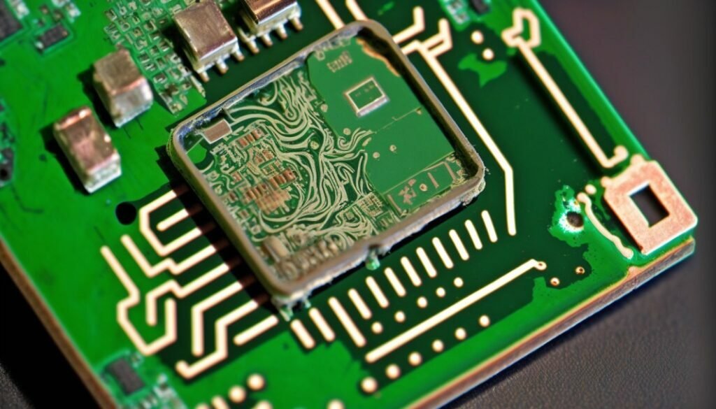
A soldering mask is a photoresist material applied to copper prepainted PCBs to protect the copper traces during the soldering process. Copper traces are exposed to heat when being soldered; if they are not covered by a solder mask, they will oxidize and corrode. The solder mask prevents this from happening to the copper traces.
A soldering mask consists of two layers: an outside layer, which is applied to the copper traces and remains on the board once soldering is complete, and an inside layer, which is applied to the outside of the board and is removed once soldering is complete. The inside layer is a photo-resist, meaning that it is sensitive to UV light and therefore unique when being applied to the photo-resist surface.
Once the mask is exposed to UV light, it changes from being soluble to insoluble, meaning it will not wash off with liquid chemicals such as ferric chloride. The outside layer is a dense, water-soluble photoresist. This makes it easy to clean off the board after soldering is complete.
Solder Mask Colors
The most popular color of solder mask is green. Of course, we can also choose others for your project, such as yellow, black, blue, red, white and so on.


How to Select the Solder Mask Color?
When selecting a solder mask color for your PCB, there are several factors to consider.
First and foremost, you must determine whether the board will be used in an indoor or outdoor setting. If the board is to be used outdoors, then a dark color such as black may be the best choice, since it is more resistant to UV radiation. On the other hand, if the board will be used indoors, then a lighter color such as green or blue is recommended, since it is easier to see markings on the board and will not attract as much dust and dirt.
Another factor to consider is the type of components being used on the board. Darker colors such as black or red tend to absorb more heat than lighter colors, so these should be avoided when using components that are heat-sensitive. Additionally, black or red may cause certain components to become too hot and cause damage.
The cost of the solder mask should also be taken into consideration. Generally speaking, darker colors are more expensive than lighter ones, so it is important to weigh the additional cost against the benefits of having a particular color.
Finally, aesthetics should be taken into account when selecting the solder mask color. For example, green may be chosen if the board is intended to be aesthetically pleasing, while black may be chosen if the board is meant to look more industrial. Ultimately, the selection of solder mask color should be based on a combination of factors to ensure that the board meets all of its requirements.
Types of Solder Mask
They are many materials for solder mask, each having their own unique properties and advantages. The most common types of solder mask materials include liquid epoxy, liquid photo imageable (LPI), dry film photo imageable (DFPI), and liquid crystal polymers (LCP).
Liquid epoxy:
Solder mask is typically made of a photosensitive liquid epoxy resin that is applied to the PCB. After the resin is dry, a UV light is used to harden the material. This process is known as “curing” and is done to ensure that the solder mask will have a good adhesion to the board and will be able to withstand environmental conditions.
Liquid Photoimageable (LPI):
The LPI solder mask is also popular, because it is relatively easy to apply and provides excellent adhesion to the PCB substrate. It is also very resistant to high temperatures, making it suitable for use with lead-free solders. Additionally, LPI solder mask allows for the precise definition of solder mask openings, allowing for greater control over soldering processes and increased yields.
Dry Film Photo Imageable (DFPI):
This type of solder mask uses a dry film photopolymer to form the protective layer on the board. This type of material is usually applied by lamination or hot air leveler, and it provides excellent adhesion and protection from environmental contaminants and oxidation. It is also easier to remove than LPI, making it ideal for repair and rework.
Liquid Crystal Polymers (LCP):
This is a relatively new type of solder mask material that is becoming increasingly popular due to its increased thermal stability and ability to provide an even, consistent coverage over the entire board. It is applied using a liquid spray and provides excellent resistance to chemicals and temperature extremes, making it ideal for outdoor applications.
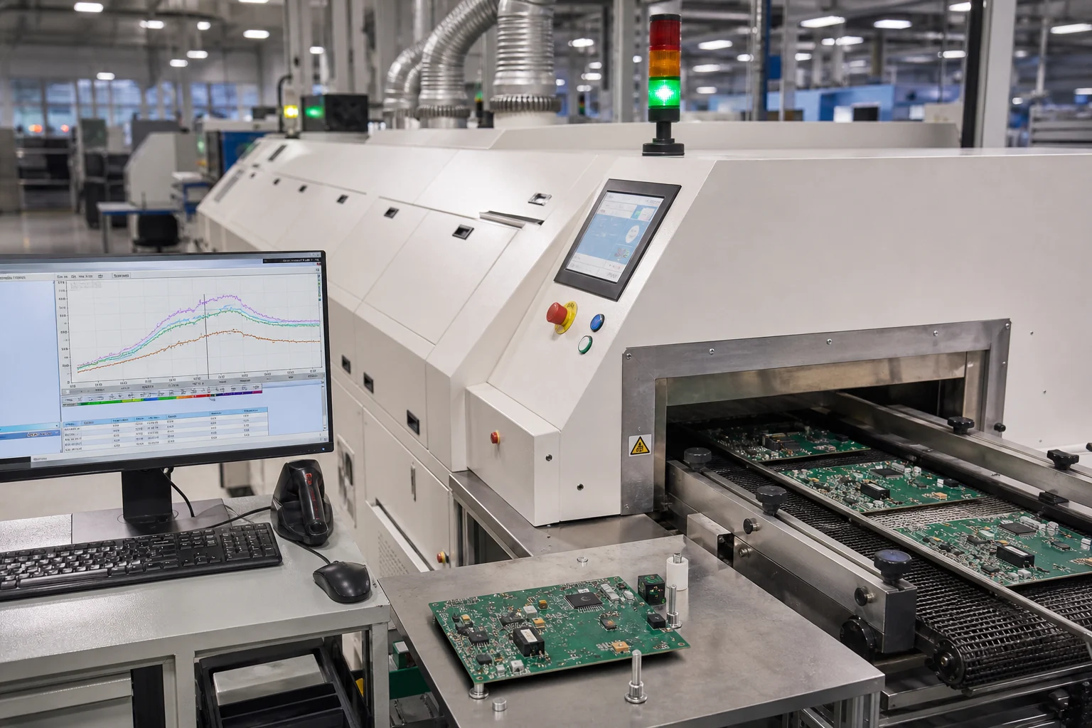
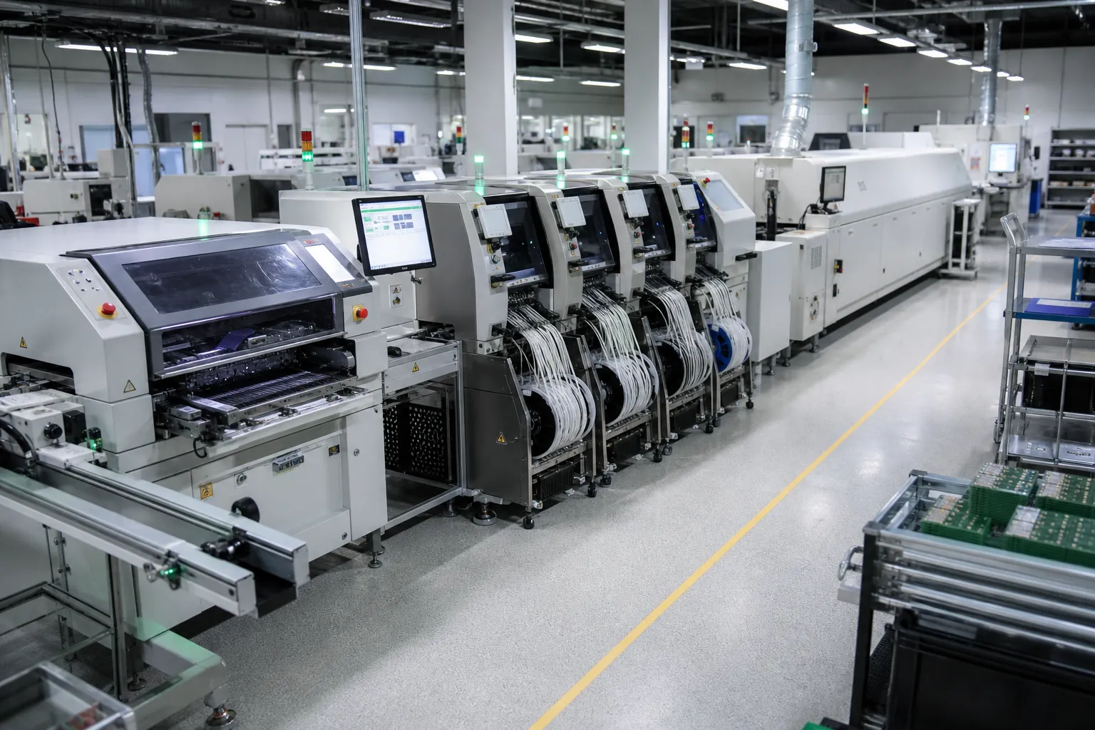
How Solder Mask is Applied?
The solder mask is typically applied using a process called screen printing. Here is how a solder mask is applied to a PCB:
- The PCB is first cleaned and prepared for the solder mask application process.
- A stencil, or screen, is created that has openings in the areas where the solder mask is desired.
- The stencil is placed onto the PCB, and a solder mask ink or paste is applied to the stencil.
- A squeegee then moves across the stencil surface, forcing the solder mask material through the openings and onto the PCB.
- The PCB is then passed through a UV light source to cure the solder mask material, making it hard and durable.
- Finally, the PCB is washed to remove any excess solder mask material that did not cure.
The end result is a PCB that has a protective layer of solder mask that prevents solder from flowing onto undesired areas, reducing the risk of short circuits and other issues. The process is repeated for multiple layers if the PCB is a multi-layered board.
Solder Mask Design Rules
Based on our best practical experience in the past, when you design the solder mask, you need to pay attention to the following points:
Tented Vias:
Tenting a via refers to covering only the annular ring of the via with solder mask, leaving the hole itself unexposed. This is a cost-effective method to protect the PCB and is preferred over more expensive techniques such as via filling or mask plugging. One of the most economical methods of via tenting is liquid photoimageable (LPI) solder mask tenting, but for better protection, resin filling can also be used at a higher cost.
Solder Mask Clearance:
The solder mask clearance, also called minimum solder mask sliver, is the minimum distance between the copper pads or traces and the edge of the solder mask opening.
In general, the solder mask clearance should be 0.075mm to 0.1mm. So that it can ensure sufficient clearance and prevent shorts between copper features. However, the specific requirements may vary depending on the PCB design, the size and spacing of the copper features, and the manufacturing process used. Some designs may require larger clearance to accommodate for the specific assembly process and the tolerances of the manufacturing equipment.
It is important to consult with your PCB manufacturer or refer to their guidelines to ensure that your solder mask clearance meets the specific requirements for your design and manufacturing process.
Solder Pads:
There are two types of pads on a PCB – solder mask defined pads and non-solder mask defined pads. Solder mask defined pads have mask openings smaller than the copper pads, which determine the pad size used in BGAs. Changes in the mask clearance affect the copper pad size. Non-solder mask defined pads have a gap between the pad and the mask. It is important to ensure that the solder mask clearance is always greater than the solder pads to prevent the mask from overlapping the pads, which could impact the soldering quality.
Solder Mask Opening:
Solder mask opening refers to the exposed circuit on the outer layers of the PCB that allows for tin (solder) to be applied. It is important to ensure that the opening is accurate to prevent unnecessary exposure of copper on the board, which could lead to corrosion and damage. Typically, solder mask openings are made to be 1:1 with the copper pads, but they can be adjusted according to the manufacturing process. The opening must be customized to the requirements to prevent exposure of the ground plane next to the pad, which could cause shorts and other issues.
Solder Mask Expansion:
Solder mask expansion is a specification in EDA software that determines the distance between the surface features and the solder mask on the board. This value can be positive, negative, or zero. Positive solder mask expansion refers to the spacing between the end of the solder mask and the outer circumference of the pad that is not covered by the mask. Zero solder mask expansion refers to the absence of any gap between the solder mask and the pad. Negative solder mask expansion occurs when the mask overlaps a region of the pad. It is important to choose the right solder mask expansion value to ensure optimal PCB performance.
Solder Mask vs Paste Mask
Solder mask and paste mask are both used in PCB manufacturing, but they serve different functions. The solder mask is a protective layer used to cover the copper traces on the PCB and prevent oxidation or other damage. In contrast, the paste mask is used in surface mount technology to show where the solder paste should be applied on the PCB. The following table shows all the compasion of them:
| Feature | Solder Mask | Paste Mask |
|---|---|---|
| Usage | protective layer for circuit board | stencil for SMD assembly and soldering process |
| Material | solder mask ink | paste |
| Size | solder mask clearance: less than 0.05mm (2mil) | stencil thickness: 0.1mm (4mil) or 0.075mm (3mil) |
| Opening | no solder mask ink | have paste |
| Colors | multicolor | gray |
Solder Mask vs Silkscreen
older mask and silkscreen are both important features on a printed circuit board. Here is a table that summarizes the differences between them:
| Feature | Solder Mask | Silkscreen |
|---|---|---|
| Function | Protective layer to prevent solder bridging and shorting | Identifies components, test points, and other features |
| Material | Epoxy-based ink or photoimageable polymer | Ink or paint |
| Color | Typically green, but can be other colors | Multiple colors available |
| Application | Applied to entire board, with openings for pads | Applied only where needed |
| Appearance | Matte finish | Glossy finish |
| Importance | Essential for board functionality | Optional but useful for assembly and maintenance |
| Location | Covers copper traces, except where pads are exposed | Applied on top of solder mask, where needed |
Overall, solder mask and silkscreen serve different purposes on a PCB, but both are important for proper assembly and maintenance of the board. Solder mask provides a protective layer to prevent solder from bridging between copper traces and shorting out the circuit, while silkscreen helps identify components and other important features.
What can I use instead of solder mask?
Solder mask is a protective layer applied on printed circuit boards to prevent solder bridges between pads and traces during the soldering process. However, in some situations, a solder mask may not be necessary, or alternative protective layers can be used instead.
Here are some alternatives to solder mask:
Kapton Tape
It is a polyimide film tape that can withstand high temperatures and is commonly used in electronic assembly. It can be applied to the areas where the solder should not go, acting as a protective barrier.
Liquid Photoimageable Solder Mask (LPSM)
It is a liquid that can be applied to the PCB to create a solder mask layer. LPSM provides better adhesion and protection compared to other types of masks.
Silkscreening
Silkscreening is a process where a layer of ink is applied on the PCB surface to mark components, text, and graphics. It can be used as a protective layer when applied to the areas where the soldering shouldn’t occur.
Solder Paste Stenciling
Stenciling solder paste on the pads before placing the components on the PCB can act as a temporary mask. The solder paste will prevent the solder from going into the areas where it shouldn’t be.
PCB Surface Finish
There are several surface finishes, such as electroless nickel immersion gold (ENIG), immersion silver, and organic solderability preservatives (OSP), which provide a protective layer on the PCB. These finishes protect the copper traces and pads from corrosion and oxidation.
Concluding Remarks
Soldering masks and copper PCBs are both common manufacturing processes. A solder mask is a technique used to keep copper traces from oxidizing. The process involves applying solder, applying a layer of photo-resistant material, and then exposing the board to UV light. It’s important to be careful when soldering PCBs to avoid these common mistakes. Using the right flux and solder, keeping the board clean and free of air, and checking the tip are all important. If you follow these tips, you should be able to solder a board properly and avoid any of these mistakes.
FAQ
No, solder mask is not conductive. In fact, it is designed to be an insulating layer that helps to protect the copper traces on a printed circuit board (PCB) from accidental contact with other conductive materials.
Yes, solder mask is a necessary component in PCB (Printed Circuit Board) manufacturing. Solder mask is a thin layer of polymer that is applied to the PCB surface, covering all the copper traces, and leaving only the pads exposed where components are mounted. The primary purpose of solder mask is to prevent solder from flowing onto unintended areas during the component soldering process.
The best solder mask for your project will depend on your specific needs and requirements. It is important to work with an experienced PCB manufacturer who can help you select the right solder mask for your project and ensure that it is applied correctly.