Selecting between selective soldering and wave soldering is usually not a theoretical exercise. It happens when a board contains through-hole content that still needs efficient soldering, but the assembly no longer behaves like a simple legacy design. Tall connectors shadow nearby parts. Bottom-side SMT components reduce clearance. Thermal mass varies from one zone to another. Operators need a process that protects already-reflowed parts without turning each job into manual touch-up. At that point, “which soldering method is cheaper?” becomes the wrong first question. The better question is which method creates the fewest escapes for the actual board mix.
Wave soldering remains productive when the assembly is compatible with conveyorized contact to a solder wave and the board design respects the process. Selective soldering becomes attractive when only certain through-hole joints need soldering or when mixed-technology geometry makes full-wave exposure too risky. Neither process is automatically better. Each one shifts the tradeoff between throughput, fixture discipline, thermal exposure, masking burden, and joint access.
ReversePCB already covers the broader wave soldering process. This article focuses on the decision point engineers actually face: when should a mixed-technology PCB stay on wave soldering, and when is selective soldering the safer or more economical choice?
What the two processes change at the board level
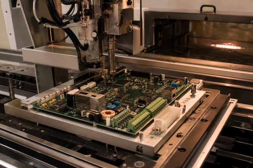
Wave soldering exposes the underside of the assembly to a continuous solder wave after fluxing and preheat. It is efficient because many joints are formed at once, but the board has to be physically compatible with that exposure. Component orientation, lead protrusion, pallet strategy, bottom-side keep-out, and solder thieves all matter. If the board was not designed for wave, the process often compensates through masking, pallet complexity, or manual rework.
Selective soldering applies solder only where needed, usually through a programmed nozzle path after controlled fluxing and preheat. That makes it better suited to mixed-technology products where only a subset of through-hole joints remain after SMT reflow. The price of that flexibility is cycle time and process programming effort. A selective process may protect the board better while producing fewer collateral problems, but it is rarely the fastest choice for a large population of simple through-hole joints.
When wave soldering still makes more sense
Wave soldering earns its place when the board has high through-hole density, compatible bottom-side geometry, and enough production volume to justify pallets or line tuning. If most of the joints need solder at once and the board can safely present those joints to the wave, the process remains efficient. It also works well when lead lengths, spacing, and orientation are consistent enough to manage bridging and drainage with established DFM rules.
The key phrase is “can safely present those joints to the wave.” Boards that were actually designed for wave usually include sensible component orientation, protected glue-down or keep-out strategy for any bottom-side SMT exposure, and clear thinking about copper imbalance near connectors or transformer pins. In that situation, wave soldering is not old-fashioned. It is simply well matched to the product.
It also remains attractive when takt time is critical and the product family is stable. A mature wave process can move a lot of assemblies with predictable operator workload, provided flux density, preheat, conveyor angle, and solder-pot conditions are tightly controlled.
When selective soldering becomes the better engineering answer
Mixed-technology boards with vulnerable bottom-side SMT
Selective soldering is often the cleaner answer when reflowed components on the underside make wave exposure risky or expensive to protect. If the board would need extensive pallet design, complicated masking, or frequent touch-up to survive the wave, the apparent productivity advantage of wave soldering starts to disappear.
Boards with only a few through-hole joints left
Some assemblies have mostly SMT content and only a small number of connectors, relays, shields, or power pins that still require hole-fill. Running the entire product through wave for that small joint count can be hard to justify. Selective soldering limits thermal and solder exposure to the necessary areas and usually reduces collateral cleaning or shielding work.
Assemblies where joint access varies significantly
Selective nozzles make it easier to treat awkward connector fields, tall housings, and mixed lead geometries as programmed process features rather than layout compromises. That does not remove the need for DFM, but it gives process engineers more control when the board is not uniformly wave-friendly.
Process risks engineers often underestimate
The usual mistake in wave soldering decisions is to count throughput and ignore rework burden. A line may look efficient until bridging, icicling, solder skips, or masked-area damage adds enough inspection and repair work to erase the gain. Boards with poor drainage paths or large thermal sinks can become especially expensive because the defect mechanism repeats consistently across panels.
The usual mistake in selective soldering decisions is to treat programming flexibility as a substitute for process discipline. Selective soldering still depends on flux placement accuracy, preheat control, nozzle maintenance, dwell control, and board support. If the nozzle path is tuned around one lot and not revalidated when component protrusion or connector housing changes, the process can quietly drift into incomplete hole-fill or overheated plastic bodies.
In both methods, the dominant risk is often upstream design mismatch. If the PCB layout never considered drainage, stand-off, thermal shadowing, and inspection access, the soldering method ends up carrying problems it was not supposed to solve.

How to compare the two methods on a real product
Start with joint population. If the board has many wave-compatible through-hole joints, wave soldering deserves a serious baseline comparison. If it has only a few critical joints embedded among SMT content, selective soldering usually enters the lead position. Then review bottom-side exposure. Any existing reflowed parts, adhesives, or low-clearance areas should be treated as cost drivers, not side notes.
Next, compare the real quality checks. Hole-fill performance, bridging rate, solder-ball behavior, connector body condition, and post-process cleaning demand tell you more than abstract cycle time. If the wave process looks faster but produces repeated repair on dense connector sections, that repair time belongs in the economic comparison. If selective soldering preserves quality but requires long programming and nozzle optimization for every revision, that engineering time belongs in the comparison too.
Finally, consider what happens after soldering. Can AOI see the critical joints? Is X-ray needed? Are operators likely to touch up the same areas repeatedly? Boards that appear acceptable immediately after soldering may still become expensive if inspection access is poor or if connector housings hide marginal fillets.
Design checkpoints that influence the answer before the line runs
Component orientation around the solder path matters. So do lead protrusion targets, pad annulus, connector body clearance, and whether heat-sensitive components sit too close to the intended solder zone. For wave processes, drainage and shadowing are central concerns. For selective processes, nozzle access and local heat concentration matter more. In both cases, fixture support and board flatness can decide whether the process window is wide or frustratingly narrow.
This is why DFM review should happen before the soldering method is locked. A minor connector rotation or keep-out adjustment can turn an awkward selective path into a stable one, or make a wave pallet unnecessary. By the time the board reaches the line, those easy wins are often gone.
Conclusion
Selective soldering and wave soldering solve different production problems. Wave soldering is strongest when the board is genuinely wave-compatible and the through-hole joint population is large enough to reward simultaneous soldering. Selective soldering is stronger when mixed-technology layouts, vulnerable bottom-side SMT, or limited through-hole populations make full-wave exposure harder to justify.
The correct choice is the one that produces acceptable joints with the least hidden cost in masking, thermal risk, inspection difficulty, and rework. If the board keeps forcing the process to work around layout realities, compare the real burden, not the simplified machine description. That is usually where the better answer becomes obvious.
What is the main difference between selective soldering and wave soldering?
Wave soldering forms many through-hole joints at once by exposing the board underside to a solder wave, while selective soldering applies solder only to programmed joint locations. The tradeoff is usually throughput versus flexibility and local control.
When is selective soldering better for a PCB assembly?
Selective soldering is usually better when the board has mostly SMT content with only a few through-hole joints, or when bottom-side SMT parts and connector geometry make wave exposure risky or expensive to protect.
Does wave soldering always cost less than selective soldering?
Not necessarily. Wave soldering can be faster, but masking, pallets, repair labor, and damage risk can erase that advantage on mixed-technology boards. The right comparison has to include defect and rework burden, not just cycle time.
What should be reviewed before choosing between the two processes?
Review through-hole joint count, bottom-side SMT exposure, connector and lead geometry, drainage paths, hole-fill requirements, fixture support, inspection access, and the expected amount of masking or programming effort.