What is Wave Soldering?
Wave soldering refers to the process of creating a desired wave-shaped solder pool using a molten solder alloy (lead-tin) through an electric or electromagnetic pump. The solder wave can also be formed by injecting nitrogen gas into the solder pool. In this process, a printed circuit board (PCB) preloaded with components is passed through the solder wave, which forms a specific shape of solder peak on the surface of the molten solder. This allows the PCB, with components mounted at specific angles and immersion depths, to be soldered through the solder wave, creating solder joints. This entire process is known as wave soldering.
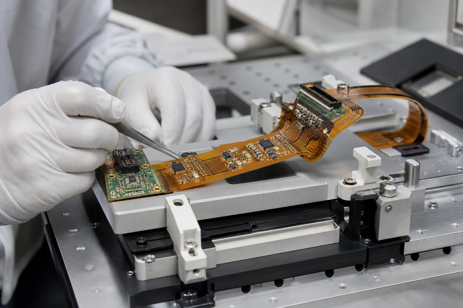
As an important step in the dual inline package (DIP) assembly process, wave soldering is primarily used for the soldering of circuit board through-hole components. Despite the trend towards miniaturization and surface mount technology (SMT), certain products such as televisions, home audio-visual equipment, and digital set-top boxes still utilize through-hole components on mixed technology circuit boards. Hence, wave soldering continues to be employed in such applications.

The History of Wave Soldering
In 1956, Fry’s Metal, a British company, invented the wave soldering method for printed circuit boards (PCBs). This innovation marked a new era of machine automation, transitioning PCB assembly from manual point-to-point soldering with soldering irons to large-scale, high-efficiency automated soldering. It truly revolutionized the soldering process for PCBs, offering significant advantages such as reduced solder joint defects, improved reliability of electronic products, lower production costs, reduced labor intensity for workers, and increased production efficiency.
How Does Wave Soldering Work?
Wave soldering is performed using a wave soldering machine, which consists primarily of a conveyor belt, soldering flux application zone, preheating zone, solder pot, and other components. Below is its’ working schematic diagram:

Conveyor Belt:
The conveyor belt transports the circuit board, with components inserted, into the wave soldering machine at a specific tilt angle and speed. The circuit board then goes through processes such as flux application, preheating, thermal compensation, the first and second wave soldering, and cooling.
Flux Application:
The flux application zone consists of infrared sensors and spray nozzles. The role of the infrared sensors is to monitor the width of the circuit board. The spray nozzles uniformly apply a thin layer of flux onto the exposed solder pads, through-hole pads, and component leads of the circuit board. The flux creates a protective film on the soldering surface of the circuit board.
Preheating:
In the preheating zone, the soldering areas of the PCB are heated to the wetting temperature. At the same time, the temperature increase of the components prevents them from experiencing excessive thermal shock when immersed in the molten solder. The surface temperature of the PCB during preheating should be controlled between 75 to 110°C to ensure proper formation of solder joints.
The purpose of preheating is as follows:
- Volatilization of solvents in the flux, reducing gas generation during soldering.
- Decomposition and activation of rosin and activators in the flux, removing oxide films and other contaminants from the solder pads, component leads, and pin surfaces of the circuit board, while protecting the metal surfaces from re-oxidation at high temperatures.
- Prevention of thermal stress damage to the PCB and components caused by rapid heating during soldering.
Thermal Compensation:
During the thermal compensation stage, the PCB undergoes thermal adjustments to reduce the impact of heat.
First Wave (Turbulent Wave):
The first wave is a narrow “turbulent” wave emitted from a narrow nozzle. The fast flow of solder allows for good penetration on soldering areas with shadowing effects from fixtures. Additionally, the upward force of the turbulent wave helps to expel solder flux gases, reducing solder bridging and insufficient vertical fill defects. However, the turbulent wave may result in uneven solder joints and excess solder, which necessitates the second wave.
Second Wave (Smooth Wave):
The second wave is a “smooth” wave characterized by slower solder flow. It effectively removes excess solder from the terminals, ensures good wetting on all soldering surfaces, and eliminates sharp edges, burrs, and solder bridges caused by the first wave. In practice, the smooth wave is similar to the traditional wave used for through-hole components. Hence, when soldering traditional components on the same machine, the turbulent wave can be turned off, and only the smooth wave is used.
Cooling:
The cooling system rapidly lowers the temperature of the PCB, significantly improving the prevention of voids and solder pad delamination issues in lead-free soldering processes.
Throughout the soldering process, the use of nitrogen gas for protection in the preheating stage and soldering zone effectively prevents oxidation of bare copper and eutectic solder, greatly enhancing wetting and flowability and ensuring reliable solder joints.
Operation Manual of Wave Soldering Machine
I. Preparations for Wave Soldering
- Power on and activate the solder pot heater (normally controlled by a timer).
- Check the timer switch of the wave soldering machine for proper functioning.
- Ensure the ventilation system of the wave soldering machine is in good condition.
- Verify the temperature indicator of the solder pot: Measure the temperature 10-15mm below the solder surface using a glass or contact thermometer. The temperature difference should be within ±5°C.
- Check the preheater for proper operation and ensure the temperature is set according to the process requirements. Turn on the preheater switch, monitor the temperature rise, and confirm it is within the normal range.
- Inspect the operation of the lead cutter: Adjust the blade height based on the PCB thickness, aiming for component lead lengths of 1.4-2.0mm. Tighten the blade holder, visually check the blade rotation after powering on, and ensure the safety device is functioning.
- Check the air supply for the flux container: Pour in the flux, adjust the air intake valve, and check if the flux foams or sprays after powering on.
- Verify the density adjustment of the flux: Check the liquid level in the flux tank and measure the density. If the density is too high, add a diluent; if it is too low, add flux to adjust (foaming).
- Once the solder temperature reaches the specified value, check the solder level. If it is below 15mm from the top of the solder pot, add solder promptly.
- Remove any solder dross from the solder surface and add an anti-oxidation agent after cleaning.
- Adjust the conveyor angle: Set the track width according to the width of the PCB to ensure appropriate clamping force.
II. Startup and Production Operation of Wave Soldering
- Turn on the flux switch. For foaming, adjust the foam thickness to half of the foam adjustment plate; for spraying, ensure a uniform coverage on the board surface without spraying the component side.
- Adjust the airflow of the air knife to allow excess flux on the board to drip back into the foam tank, preventing it from dripping onto the preheater and causing a fire.
- Activate the conveyor switch and adjust the speed to the desired value.
- Turn on the cooling fan.
III. Post-Soldering Operation for Wave Soldering
- Turn off the switches for the preheater, solder pot, flux, conveyor, cooling fan, and lead cutter.
- The flux in the foam tank should be replaced every two weeks, and regular measurements should be taken during usage.
- Clean the wave soldering machine and chain claws after shutdown. Soak and clean the spray nozzles with a diluent.
IV. Management Methods during the Wave Soldering Process
- Operators must remain at their posts and regularly inspect the equipment’s operation.
- Operators should check the quality of solder joints. In the event of any abnormalities, the machine should be stopped immediately for inspection.
- Timely and accurate records should be kept of the original operation data and solder joint quality.
- Completed PCB boards should be separately placed in dedicated transport boxes, avoiding contact, pressure, and stacking.
V. Operation Records for Wave Soldering
The wave soldering operator should record process parameters such as solder pot temperature, preheating temperature, and flux density every two hours. Additionally, 10 PCB boards should be randomly inspected and the solder joint quality should be recorded every hour, providing original records for process quality control.
Advantages of Wave Soldering
- Labor and material savings: It improves production efficiency and reduces manufacturing costs.
- Reduced board warping: The short contact time of the circuit board with high-temperature solder minimizes board distortion.
- Elimination of human factors: It eliminates interference and impact on product quality, resulting in improved solder joint quality and reliability.
- Enhanced solder activity: The wave soldering machine ensures sufficient solder movement, leading to better solder joint quality.
- Improved working environment: The adoption of a good exhaust system improves the operator’s physical and mental well-being.
- Oxidation prevention: The surface layer of the solder forms a protective barrier against oxidation, reducing solder wastage caused by oxidation residue.
- Consistency: It ensures consistent product assembly quality and standardized processes.
- Ability to handle tasks beyond manual capabilities.
Engineering checks for Wave Soldering Guide: Process & Best Practices
Before using Wave Soldering Guide: Process & Best Practices in a PCB, firmware, repair, or validation workflow, confirm the details that usually decide whether the design works reliably instead of only reading the headline specification.
Design and troubleshooting checklist
| Area | What to check | Why it matters |
|---|---|---|
| Pinout and package | Verify the wave soldering diagram pinout, package variant, polarity, and footprint before assembly | Similar packages can have different pin order or exposed-pad rules |
| Electrical limits | Check voltage, current, power, frequency, thermal rating, and derating | Headline ratings rarely apply in every PCB condition |
| Substitution | Compare datasheets, markings, tolerances, and circuit role before replacing parts | Equivalent parts still need board-level evidence |
These checks help connect the search intent around wave soldering diagram with practical board-level decisions, component selection, and failure analysis.
Wave Soldering vs. Reflow Soldering
Welding processes play a crucial role in electronic device manufacturing as the quality of soldering directly affects product performance and lifespan. Among various welding methods, reflow soldering and wave soldering are the two most common techniques, each with its own characteristics and applications.
Wave Soldering:
Wave soldering is mainly used for through-hole components (THT). In this method, the PCB with components passes over a molten wave of solder, creating solder joints between the component pins and PCB.
Characteristics of Wave Soldering:
- High efficiency: Similar to reflow soldering, wave soldering can handle all components on a PCB simultaneously, ensuring high efficiency.
- Suitable for large-sized and high-power components: Wave soldering uses more solder than reflow soldering, providing stronger mechanical support and electrical connections, making it suitable for larger-sized and high-power components.
- High automation: Wave soldering, like reflow soldering, can be fully automated, minimizing the influence of human factors on soldering quality.
Reflow Soldering:
Reflow soldering is primarily used for surface mount components (SMT). In this method, the printed circuit board (PCB) with solder paste and components is heated in a controlled temperature environment. The solder paste melts and solidifies, completing the soldering process.
Characteristics of Reflow Soldering:
- High efficiency: Reflow soldering can handle all components on a PCB simultaneously, significantly improving production efficiency.
- High quality: As the soldering process takes place in a tightly controlled temperature environment, the solder joints are typically of high quality, ensuring reliability and good joint formation.
- Suitable for high-density and small components: Reflow soldering is ideal for soldering high-density and small components, including BGA and QFP, as it does not involve direct contact with the components.
- High automation: Reflow soldering is often fully automated, reducing human errors and increasing production efficiency.
Selection between Wave Soldering and Reflow Soldering
When choosing a soldering method, the following factors are usually considered:
- Component type: Reflow soldering is preferred for surface mount components (SMT), while wave soldering is commonly used for through-hole components (THT).
- Component density and size: Reflow soldering is more suitable for high-density and small components, while wave soldering is better for larger-sized and high-power components.
- Production efficiency: Both reflow soldering and wave soldering offer high efficiency when fully automated.
- Quality requirements: If strict soldering quality is required, reflow soldering in a tightly controlled temperature environment is recommended.
In summary, reflow soldering and wave soldering each have their advantages. The choice between them depends on specific product requirements and production conditions. The electronics manufacturing industry is constantly evolving, and with the emergence of new welding technologies and equipment, continuous learning and adaptation are essential to meet evolving production needs
Wave Soldering vs Selective Soldering
Selective wave soldering, also known as selective soldering, is different from traditional wave soldering. In traditional wave soldering, the entire surface of the PCB is coated with flux, and during soldering, the PCB’s soldering surface is fully immersed in molten solder. However, selective wave soldering is different. It allows for setting soldering parameters for each individual solder joint on the PCB, such as flux spraying position, soldering time, and wave height. This means that selective wave soldering can apply flux only to the solder points, avoiding unnecessary flux application and ensuring that only the soldering area comes into contact with the solder.
The advantages of selective wave soldering include:
- Reduced flux usage: By selectively applying flux only to the solder points, the consumption of flux is minimized. This not only saves costs but also reduces the generation of flux residues.
- Lower solder consumption: Since only the soldering area comes into contact with the solder, selective wave soldering reduces solder usage.
- Reduced solder dross: With selective wave soldering, the occurrence of solder dross is minimized due to the focused soldering process.
- Compact size and versatility: Selective wave soldering machines are compact and come with a built-in worktable, allowing them to adapt to various PCB shapes. This eliminates the need for multiple fixtures and saves equipment space.
However, there are also some disadvantages to selective wave soldering:
- Higher cost: Selective wave soldering equipment tends to be more expensive compared to traditional wave soldering machines due to its advanced technology and capabilities.
- Lower efficiency: As each solder joint requires specific programming and control, the efficiency of selective wave soldering is relatively lower compared to traditional wave soldering.
Overall, selective wave soldering offers several advantages such as reduced flux usage, lower solder consumption, and compact size. However, it comes at a higher cost and lower efficiency compared to traditional wave soldering due to its specialized nature and advanced technology.
The Development Trends of Wave Soldering
With the widespread adoption of surface mount technology (SMT) replacing through-hole components, wave soldering has been largely replaced by reflow soldering in many large-scale electronic applications. However, there is still a significant demand for wave soldering in certain areas where SMT is not suitable, such as large power devices, high-pin-count connectors, or in industries where simple through-hole technology dominates.
Despite the increasing application of other soldering methods, such as selective soldering, wave soldering still maintains its unique advantages, which make it a viable choice for PCB assembly.