Definition of Printed Circuit Board
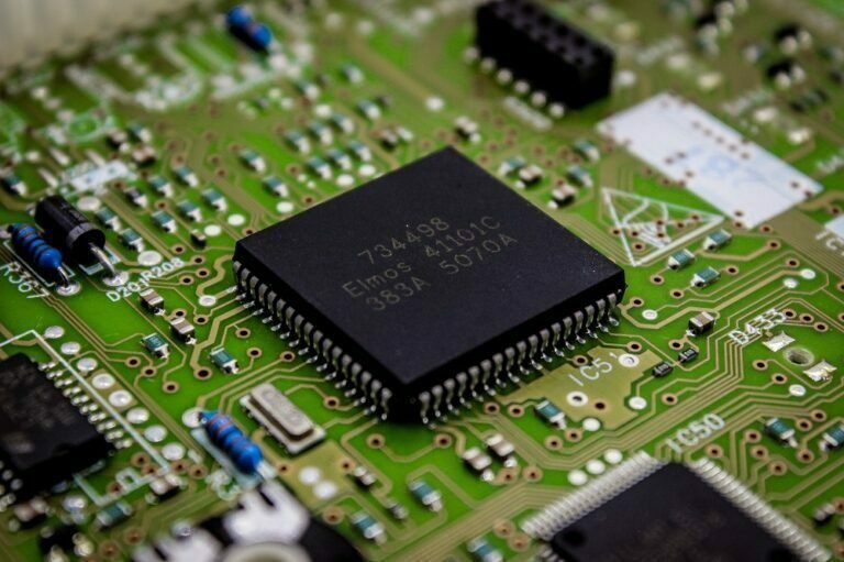
PCB (Printed Circuit Board) is the support body for electronic components and circuit connections. Because it is made by electronic printing technology, it is called a printed circuit board. It transfers the circuit to the substrate by means of image transfer, and generates the circuit after chemical etching.
The Origin of PCBs
In 1925, Charles Ducas from the United States, the founder of the additive method, printed circuit patterns on insulated substrates, and then successfully produced conductors using electroplating.
In 1936, Paul Eisler from Austria, the founder of the subtractive method, first used a printed circuit board in a radio.
In 1943, the United States applied this technology to military radios. In 1948, the United States officially recognized this invention for commercial use.
Since the mid-1950s, printed circuit boards have been widely used in the electronics industry and have since become dominant. PCBs have developed from single-layer to double-sided, multi-layered, and flexible, each with its own development trend. With the continuous development towards high-precision, high-density, and high-reliability, as well as a reduction in size, cost, and improved performance, printed circuit boards still maintain strong vitality in the future development of electronic devices.
Functions of PCBs
PCBs have the following functions in electronic devices:
- They provide mechanical support for various electronic components such as integrated circuits, and enable wiring and electrical connections or insulation between various electronic components. They also provide the required electrical characteristics.
- They provide solder mask graphics for automatic soldering, and identification characters and graphics for component insertion, inspection, and repair.
- The use of PCBs in electronic devices avoids wiring errors and enables automated component insertion or surface mounting, automatic soldering, and automatic testing. This ensures product quality, improves labor productivity, reduces costs, and facilitates maintenance.
- They provide the required electrical characteristics, characteristic impedance, and electromagnetic compatibility for high-speed or high-frequency circuits.
- PCBs with embedded passive components provide certain electrical functions, simplify the electronic installation process, and improve product reliability.
- They provide an effective chip carrier for miniaturized chip packaging in large-scale and ultra-large-scale electronic packaging components.
Different Types of PCBs
There’re many different classification methods for PCB, including substrate material, structure characteristic, number of layers, application, etc.
Substrate material
PCB substrate refers to the base material used to create a printed circuit board (PCB). It provides the foundation for the circuitry and components that make up an electronic device. PCB substrates are typically made from a variety of materials, including fiberglass-reinforced epoxy resin (FR-4), polyimide, and ceramic.
| PCB Substrate Type | Examples |
|---|---|
| Paper-based PCBs | Phenolic Paper-based PCBs, Epoxy Paper-based PCBs, etc. |
| Glass Cloth-based PCBs | Epoxy Glass Cloth-based PCBs, PTFE Glass Cloth-based PCBs, etc. |
| Synthetic Fiber-based PCBs | Epoxy Synthetic Fiber-based PCBs, etc. |
| Organic Thin Film-based PCBs | Nylon Thin Film-based PCBs, etc. |
| Ceramic Substrate-based PCBs | - |
| Metal Core-based PCBs | - |
Structure Characteristic
According to the structural characteristics, PCB can be divided into rigid circuit board, flexible circuit board and soft and hard combination board. The difference in appearance between rigid PCB and flexible PCB is that flexible PCB can be bent.

- Common thicknesses of rigid PCBs are 0.2mm, 0.4mm, 0.6mm, 0.8mm, 1.0mm, 1.2mm, 1.6mm, 2.0mm, etc.
- The common thickness of the flexible PCB is 0.2mm, and the place where the parts are to be soldered will be added with a thickened layer behind it. The thickness of the thickened layer varies from 0.2mm to 0.4mm.
- Common materials for rigid PCBs include: phenolic paper laminates, epoxy paper laminates, polyester glass felt laminates, epoxy glass cloth laminates.
- Common materials for flexible PCBs include: polyester film, polyimide film, and fluorinated ethylene propylene film.
Number of Layers
According to the number of layers, printed circuit boards can be divided into single-sided boards, double-sided boards, multi-layer boards and HDI boards (high-density interconnect boards).
Single Sided PCB
A single-sided board refers to a circuit board that is wired on only one side (soldering side) of the circuit board, and all components, component labels and text labels are placed on the other side (component side).
The biggest feature of the single-sided panel is its low price and simple manufacturing process. However, since the wiring can only be carried out on one surface, the wiring is more difficult, and the wiring is prone to failure, so it is only suitable for some relatively simple circuits.

Double Sided PCB
The double-sided board is wired on both sides of the insulating board, one side is used as the top layer, and the other side is used as the bottom layer. The top and bottom layers are electrically connected through vias.
Usually, components on a two-layer board are placed on the top layer; however, sometimes components can be placed on both layers in order to reduce the size of the board. The double-layer board is characterized by moderate price and easy wiring. It is the most commonly used type in ordinary circuit boards.

Multilayer PCB
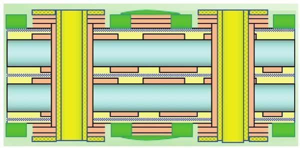
A printed circuit board with more than two layers is called a multilayer board, such as 2 layer, 4 layer, 6 layer, 8 layer, etc.
Application
- Consumer PCBs: toys, cameras, televisions, audio equipment, mobile phones, etc.
- Industrial PCB: security, automobile, computer, communication machine, instrumentation, etc.
- Military PCB: aerospace, drones, radar, etc.
PCB Structure
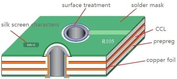
PCB is mainly composed of copper clad laminates (CCL), prepreg (PP sheet), copper foil, solder mask. At the same time, in order to protect the exposed copper foil on the surface and ensure the welding effect, it is also necessary to carry out surface treatment on the PCB, and sometimes it is also marked with characters.
The schematic diagram of the PCB four-layer board structure is shown in the figure:
Copper Clad Laminate
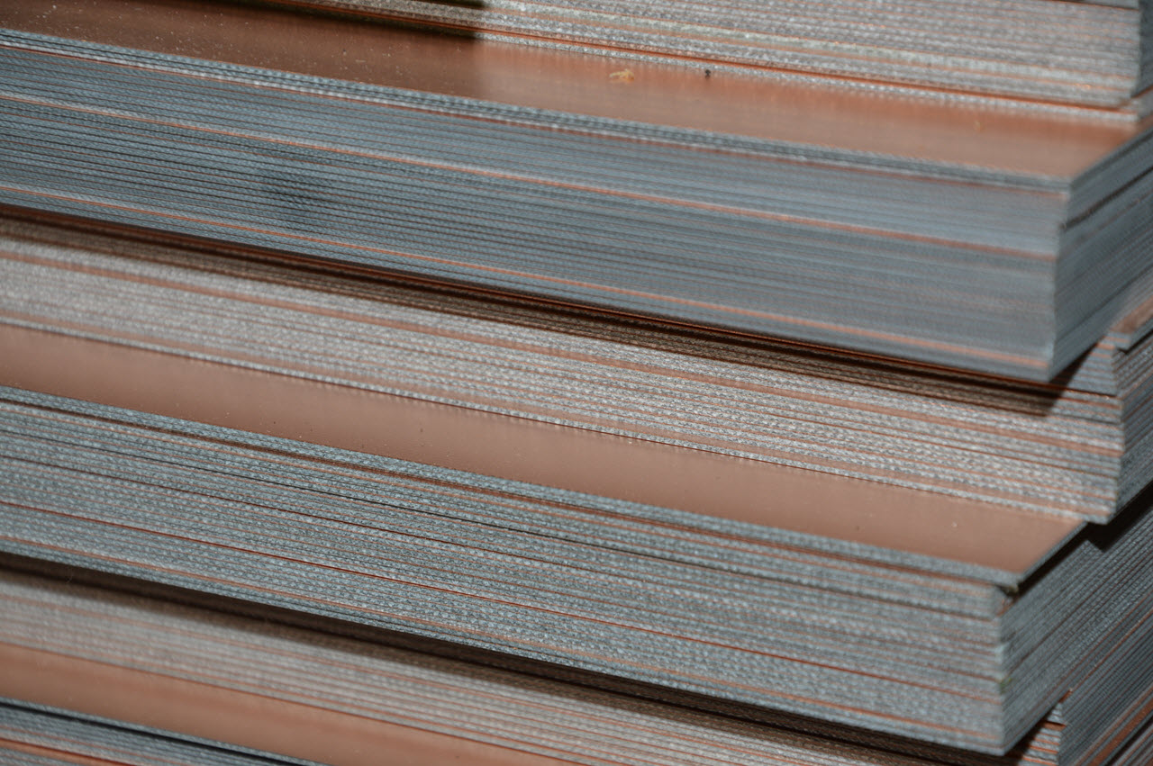
Copper-clad laminate (CCL), is the basic material for manufacturing printed circuit boards. It is composed of a dielectric layer (resin, glass fiber) and a high-purity conductor (copper foil). composed of composite materials.
Prepreg
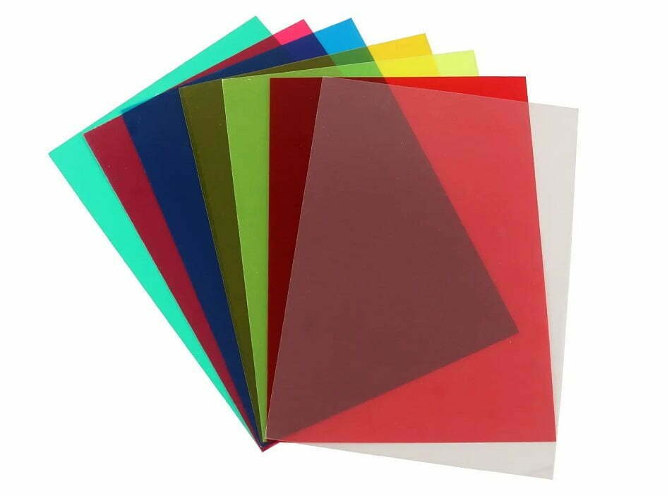
Prepreg, also known as PP sheet, is one of the main materials in the production of multilayer boards. It is mainly composed of resin and reinforcing materials. The reinforcing materials are divided into glass fiber cloth (referred to as glass cloth), paper base and composite materials.
Most of the prepregs (adhesive sheets) used in the production of multilayer printed circuit boards use glass cloth as a reinforcing material. The thin sheet material made by impregnating the treated glass cloth with resin glue, and then pre-baked by heat treatment is called prepreg. Prepregs soften under heat and pressure and solidify when cooled.
Copper Foil
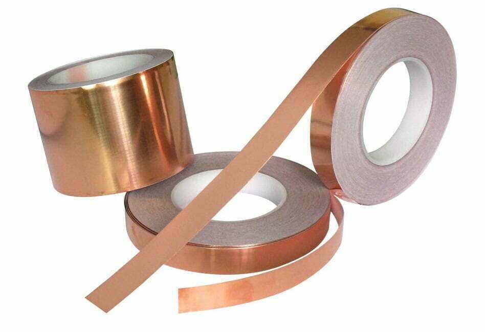
Copper foil is a thin, continuous metal foil deposited on the base layer of the circuit board. As a conductor of the PCB, it is easily bonded to the insulating layer and etched to form a circuit pattern.
Solder mask
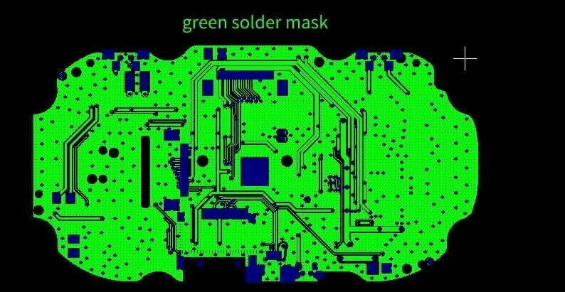
The solder resist layer refers to the part of the printed circuit board with solder resist ink. It is a permanent protective layer of the printed circuit board and can play the role of moisture-proof, anti-corrosion, anti-mildew and mechanical abrasion. Solder resist ink is usually green, and a few use red, black and blue, etc., so solder resist ink is often called green oil in the PCB industry. It can also prevent parts from being soldered to incorrect places.
PCB Production Process
The production process of PCB (Printed Circuit Board) typically includes the following steps:
Material cutting:
The raw copper-clad material is cut into the required size for the PCB board.
Layout:
The graphic file provided by customer is laid out to determine the position of components and routing on the PCB board.
Film printing:
Import and modify the layout file in software, and then print it onto a black film made of silver salt photosensitive glue. This film is used for precise positioning of components on the PCB board.
Exposure:
Apply the photosensitive liquid to the surface of the PCB board, then place the film over the board and expose it to UV light. After exposure, the film is removed, leaving only the required lines and component positions on the PCB board.
Etching:
Immerse the PCB board in etching solution to remove unwanted copper foil and retain the required circuitry and component positions. The etching process usually includes steps such as developing, etching, and stripping. The etching method differs for inner and outer layer PCB boards.
Drilling:
Drill holes on the PCB board, according to the size and coordinates of the through-hole in the file. Non-metallic holes may require dry film or two drilling or plug-hole methods.
Plating:
Place the PCB board in an electroplating bath containing chemical copper, allowing a thin layer of copper to deposit on the non-conductive substrate and the copper surface to ensure conductivity.
Solder mask and silkscreen printing:
To protect the circuit and components from oxidation and corrosion, we need to apply the solder mask on the PCB board. Normally, the common solder mask is green, you can choose vary from multi-colors according to your requirement. On th surface of PCB and solder mask, you can also print the characters, marking, symbols and labels.
Final inspection:
Run a series of test, such as AOI, ERC, to ensure that the PCB meets customer requirements and standards.
PCB Vs IC
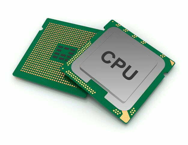
The primary distinction between PCB and IC lies in the fact that while a PCB board serves as a platform for the integrated circuit (IC), the IC is affixed to the PCB board via soldering. Below is a comparison table highlighting their differences.
| Criteria | PCB | IC |
|---|---|---|
| Definition | Printed Circuit Board | Integrated Circuit |
| Function | Provides a mechanical support for electronic components and interconnects them. | Contains multiple electronic components and their interconnections on a single piece of silicon, providing a complete electronic circuit function. |
| Size | Can vary greatly in size, from a few square millimeters to several meters. | Typically very small, with dimensions ranging from a few millimeters to a few centimeters. |
| Complexity | Can be simple or complex depending on the application. | Can be highly complex, with millions of transistors and other components integrated onto a single chip. |
| Manufacturing | Fabricated using various processes including drilling, etching, plating, and soldering. | Fabricated using semiconductor manufacturing processes including lithography, deposition, and diffusion. |
| Cost | Generally less expensive than ICs for simpler applications. | Generally more expensive than PCBs due to the complexity of the manufacturing process. |
| Reliability | More susceptible to failure due to external factors such as vibration, thermal cycling, and moisture. | Generally more reliable than PCBs due to their monolithic nature, but can still be susceptible to failure due to manufacturing defects or external factors. |
| Applications | Used in a wide range of electronic devices, including computers, televisions, and appliances. | Used in a wide range of electronic devices, including computers, mobile phones, and automotive electronics. |

