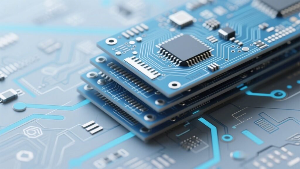
What is PCB Substrate?
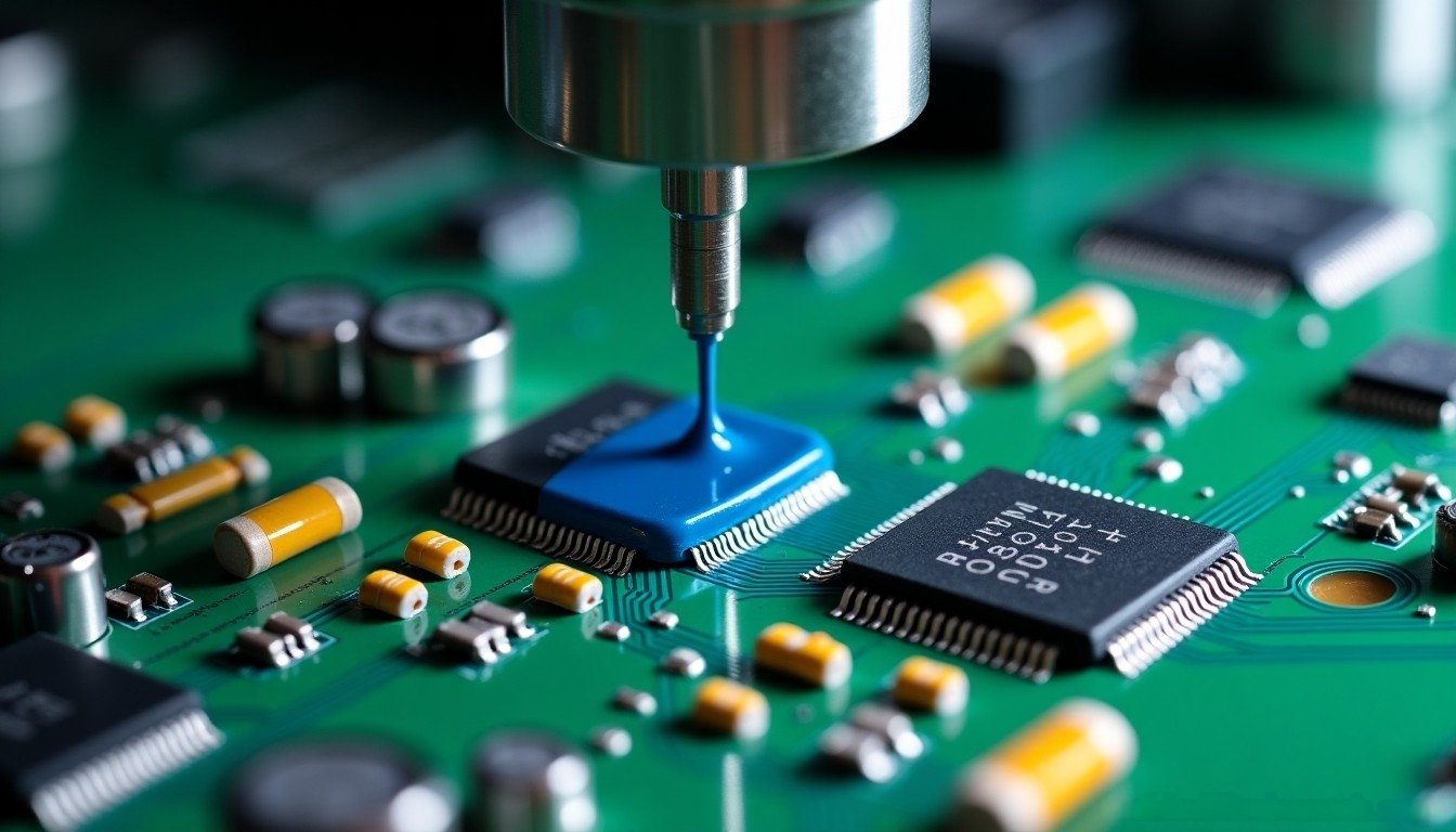
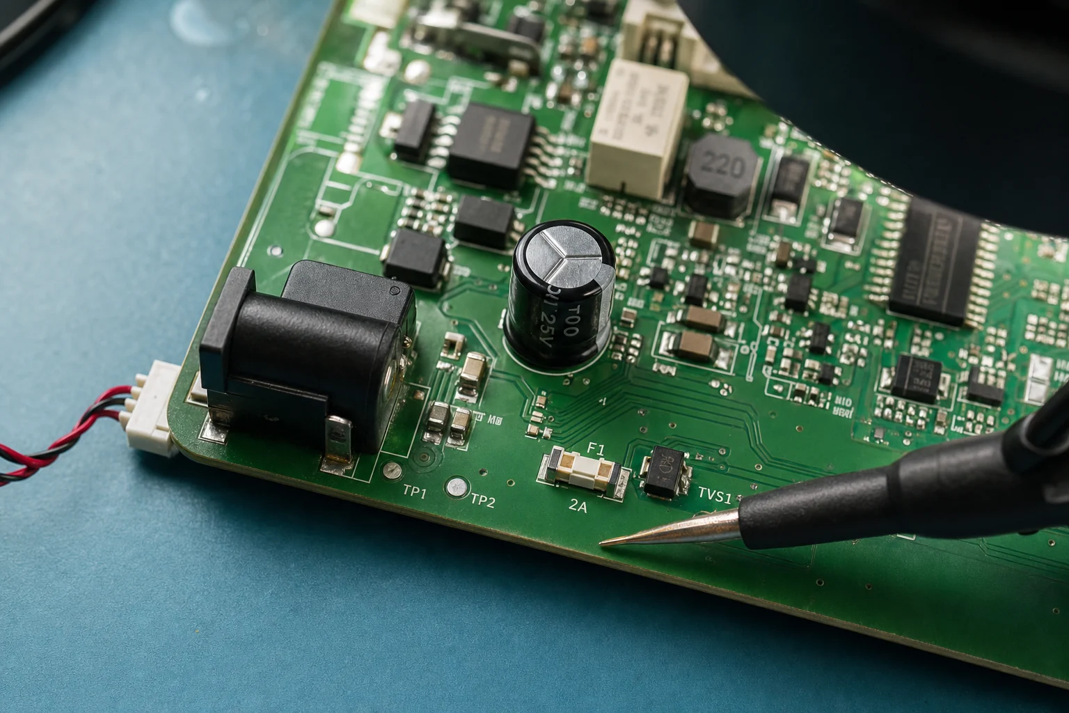
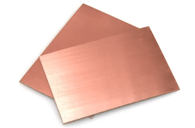
PCB substrate is the fundamental material used in the manufacturing of printed circuit boards (PCBs). Typically, the substrate is a copper-clad laminate (CCL), which is selectively processed with techniques such as drilling, chemical copper plating, electroplating, and etching to obtain the desired circuit pattern for single-sided or double-sided PCBs. The substrate serves the functions of conductivity, insulation, and support. The performance, quality, processing during manufacturing, manufacturing cost, and level of manufacture of PCBs are heavily dependent on the substrate material.
History of PCB Substrate Development
The technology and production of substrate materials have undergone half a century of development, with the global annual production reaching 290 million square meters, driven by the innovative developments in electronic products, semiconductor manufacturing technology, electronic assembly technology, and PCB technology.
Since the practical use of copper-clad laminate boards made from phenolic resin-based substrates in 1943, the development of substrate materials has been very rapid.
In 1959, Texas Instruments produced the first integrated circuit, which raised the requirement for higher-density assembly of PCBs, promoting the creation of multilayer boards.
In 1961, Hazeltine Corporation in the United States successfully developed the technology of multilayer boards using the metalization through-hole process.
In 1977, BT resin achieved industrial production, providing a new type of substrate material with high and low Tg for the development of multilayer boards worldwide.
In 1990, IBM in Japan announced a new technology for multilayer boards using a layer stacking method with photosensitive resin as the insulating layer.
In 1997, the high-density interconnect multilayer board technology, including layer-stacked multilayer boards, entered a mature development phase. Meanwhile, plastic packaging substrates, represented by BGA and CSP, have had rapid development. In the late 1990s, new types of substrates, such as green flame retardant substrates without bromine and antimony, rapidly emerged and entered the market.
Different Types of PCB Substrate Materials
Printed circuit boards can generally be classified into two categories based on substrate materials: rigid substrate materials and flexible substrate materials. The most important variety of rigid substrate materials is copper-clad laminate (CCL), which is made by reinforcing material immersed in resin adhesive, dried, cut, laminated, and then covered with copper foil. It is formed under high temperature and pressure using a steel plate as a mold in a hot press. Semi-cured sheets of CCL, mainly made from resin-impregnated glass cloth, are used to produce most multi-layer boards.
| Substrate Material | Description |
|---|---|
| Rigid Substrates | Non-flexible materials that withstand high temperatures and pressures. |
| Copper-Clad Laminate (CCL) | The main rigid substrate made by laminating copper foil onto resin-impregnated reinforcement material. |
| Flexible Substrates | Thin, lightweight materials that can bend or fold. |
| Reinforcement Materials | Paper, glass fiber cloth, composite-based (CEM series), and special materials (ceramic, metal core, etc.). |
| Resin Types | Phenolic, epoxy, polyester, and others. |
| Flame-Retardant Types | UL94-V0 (flame-retardant) and UL94-HB (non-flame-retardant). |
| Environment-Friendly CCL | Flame-retardant CCL without brominated compounds. |
| Performance-Based | General, low Dk, high heat-resistant (>150°C), low expansion CCLs, and others. |
Factors to Consider When Choosing PCB Substrate Material
You might ask what factors should be considered when selecting the PCB substrate. Well, it’ll depends on the application of your circuit board. But there’re some important material characteristics that would affect the performance of your PCB. You should consider them before make a decision.
Dielectric constant
This is the primary electrical characteristic to consider when designing laminates for high-speed/high-frequency PCBs. The dielectric constant is a complex quantity that is a function of frequency and causes dispersion in PCB substrates in the following forms:
Velocity dispersion: Because the dielectric constant is a function of frequency, different frequencies will experience different levels of loss and propagate at different speeds.
Loss dispersion: The attenuation experienced by a signal is also a function of frequency. A simple model of dispersion suggests that loss increases with increasing frequency, but this is not strictly correct, and there may be complex relationships between loss and the frequency spectrum in some laminates.
Both of these effects contribute to the degree of distortion a signal experiences during propagation. Dispersion is irrelevant for analog signals operating in very narrow bandwidths or at a single frequency. However, it is critical for digital signals and is one of the primary challenges in modeling high-speed digital signals and designing interconnects.
Glass weave style
The glass weave style creates gaps on the PCB substrate, which is related to the resin content on the board. The combination of the volume ratio of glass and impregnation resin determines the volume-averaged dielectric constant of the substrate. Additionally, gaps in the glass weave style produce a phenomenon called fiber weave effect, where the substrate dielectric constant varies along the interconnect line, causing skew, resonance, and losses. These effects become prominent at around 50 GHz or higher frequencies, affecting radar signals, gigabit Ethernet, and typical LVDS SerDes channel signals.
Copper roughness
Although this is actually a structural characteristic of printed copper conductors, it contributes to interconnect impedance. Surface roughness of the conductor effectively increases its skin effect resistance at high frequencies, resulting in eddy currents induced during signal propagation, causing loss. Copper etching, copper deposition methods, and the surface of the prepreg all affect surface roughness to some extent.
Thermal conductivity and specific heat
The amount of heat required to raise the temperature of the board by one degree is quantified by the specific heat of the substrate, while the amount of heat transmitted through the board per unit time is quantified by thermal conductivity. These PCB material properties jointly determine the final temperature of the circuit board when it reaches thermal equilibrium with its environment during operation. If you deploy your circuit board in an environment that requires rapid dissipation of heat to a large heatsink or enclosure, you should use a substrate with higher thermal conductivity.
Glass transition temperature and coefficient of thermal expansion (CTE)
These two PCB material characteristics are also related. All materials have a coefficient of thermal expansion (CTE), which is precisely the anisotropic quantity in PCB substrates (i.e., the expansion rate is different along different directions). Once the temperature of the circuit board exceeds the glass transition temperature, the CTE begins to play a role, affecting the reliability of the board. Therefore, it is important to select a substrate with an appropriate glass transition temperature and CTE that meets the environmental requirements of the PCB.