What is ODB++?
ODB++ is an open, hierarchical data structure for printed circuit board (PCB) design data and is widely used in the electronics industry. It is a comprehensive format that includes all the information needed to manufacture a PCB, such as layer stack-up information, netlists, drill files and artwork. ODB++ was developed by Valor Computerized Systems in the late 1980s and has since become an industry standard.
ODB++ Structure
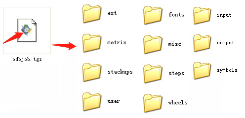
The ODB++ structure consists of several components. At the highest level, these include the header, which contains general information about the design; the layers, which include data on all of the layers in the board; the components, which include information on all the parts used in the board; and the nets, which include information on how the components are connected. Each of these components is further broken down into subcomponents. For example, the layers component may contain information about individual copper layers, dielectric layers, solder masks, and so on. The components may contain information about part numbers, board locations, and even 3D models. And the nets may contain information about netlist connectivity, trace lengths, and other routing data.
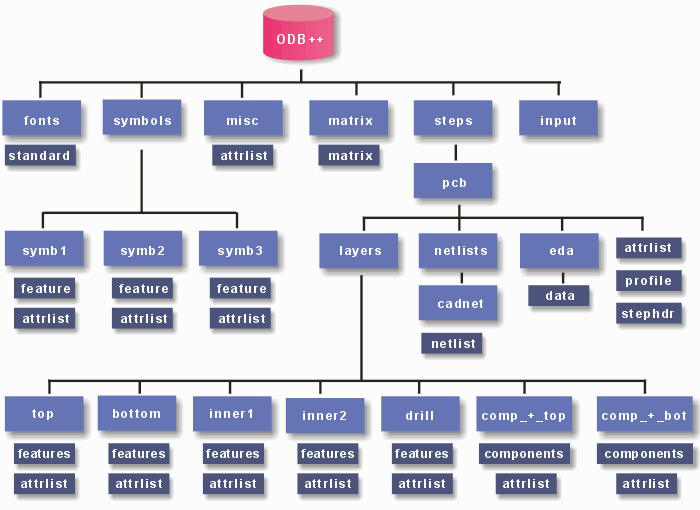
By combining all of these pieces of information into one unified structure, ODB++ ensures that all the data necessary for manufacturing a PCB is conveyed in a single file. This makes it easier for software to interact with the data and helps reduce errors and omissions. In addition, the hierarchical structure of ODB++ makes it easy to add new features and enhancements over time, ensuring that designs stay up to date with the latest technologies.
ODB++ Package Preflight for PCB Test and CAM Handoff
An ODB++ file is an intelligent PCB manufacturing package, not merely a stack of plotted layers. Before CAM review or ODB++ file testing services, verify that the archive preserves its job, step, matrix, feature, net, component and attribute data as one revision-controlled dataset.
- Check archive identity: extract the package without errors and confirm the intended job, board step and revision; remove accidental duplicate or obsolete jobs.
- Verify the matrix: review layer names, types, order, polarity, units, origin and board profile so copper and non-copper data cannot be misclassified.
- Audit fabrication features: confirm copper, mask, paste, plated and non-plated drills, slots, routes and any controlled-depth operations.
- Preserve design intelligence: compare net names, component references, package names and pin mappings with the approved schematic, BOM and placement data.
- Run acceptance checks: compare the extracted and CAD netlists, investigate every open or short discrepancy, and bind DFM and test reports to the same revision identifier.
How to Output ODB++ in Allegro?
Step 1: you need to install the ODB++ inside for the Cadence Allegro Design software.

Step 2: Select “Tools>Database Check” from the menu in turn.
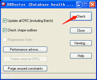
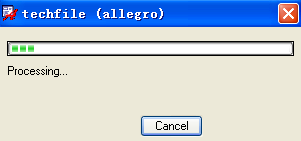
Step 3: Select “File>Export>ODB++ inside” to output the board layer information according to the tech file.
Step 4: Then select the “GZIP” option, so that the output data will be automatically compressed into a single file.
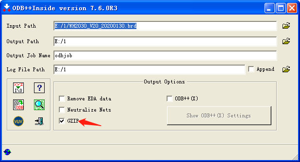
Step 5: Then when you click the ODB icon, the following pop-up window will appear.
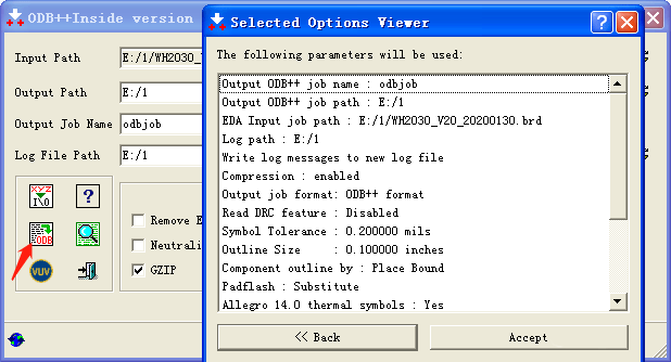
Step 6: Then click “Accept” to start outputting the file, and finally wait for the successful message to appear in the window.
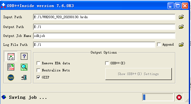
Step 7: At last, we output and decompress the “odbjob.tgz” file.