PCBA manufacturing does not start at the stencil printer. By the time a panel reaches paste printing, many yield risks have already been decided by the BOM, package assumptions, approved alternates, fixture access, and the way the assembler is expected to verify the first build. A smooth SMT line can expose those weaknesses quickly, but it rarely fixes them by itself.
For engineers and sourcing teams, the useful question is not simply whether a supplier can assemble the board. The better question is whether the release package gives production enough information to repeat the build without guessing. That is where quote-ready jobs often separate into two groups: boards that move into a controlled process window, and boards that spend the first lot absorbing preventable corrections.
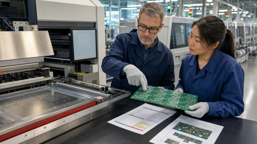
Before the Line Starts, the Data Package Has Already Set the Risk Level
A PCBA package can look complete while still leaving manufacturing with open decisions. Gerbers, ODB++ data, centroid files, a BOM, and an assembly drawing are only useful when they agree with each other. If the BOM calls a part by an internal number, the centroid file uses a footprint name that no one recognizes, and the drawing does not mark polarity clearly, the assembler has to resolve engineering decisions during production preparation.
The first review should therefore read the job like a manufacturing instruction set, not like a document checklist.
- Manufacturer part numbers need to be explicit. Distributor-only references and house numbers create avoidable confusion when availability changes.
- Package names need to match the land pattern. A label such as “QFN32” is not enough if the exposed pad, pitch, thermal slug, or body size can vary between suppliers.
- Polarity and orientation should be visible before programming. LEDs, electrolytics, diodes, connectors, and asymmetric IC packages still cause escapes when drawings rely on tribal knowledge.
- Alternates need assembly approval, not only electrical approval. A substitute part may meet the circuit requirement while changing nozzle choice, feeder setup, stencil behavior, inspection visibility, or rework risk.
This is why ReversePCB’s design-for-manufacturing workflow treats PCBA manufacturing as a release-quality problem before it becomes a soldering problem. The earlier those decisions are locked down, the less the SMT line has to interpret under schedule pressure.
Material Readiness Is More Than Having Parts in the Building
A fully kitted job can still be fragile. The purchasing team may have every line item on site, but production still needs parts in a condition and format that match the chosen assembly method. The difference matters most in low-volume and NPI builds, where short reels, mixed packaging, last-minute substitutions, and incomplete moisture handling rules are common.
Moisture, packaging, and feeder assumptions
MSL-sensitive packages need floor-life control and baking decisions before they are opened near the line. Cut tape may be acceptable for a prototype, but it can slow feeder setup or increase handling damage when the part is small, polarized, or expensive. Loose-pack parts may require manual placement, and that changes the inspection plan. These are not administrative details; they change how repeatable the first build can be.
Stencil and panel assumptions
Stencil strategy should reflect the actual package mix. Fine-pitch ICs, bottom-terminated components, large thermal pads, and 0201 passives rarely share the same ideal aperture behavior. Panel design also affects the run: thin boards, odd outlines, weak break-off tabs, and poor rail support can turn a good paste print into a handling problem before reflow begins.

The Four Controls That Keep a PCBA Build Inside Its Process Window
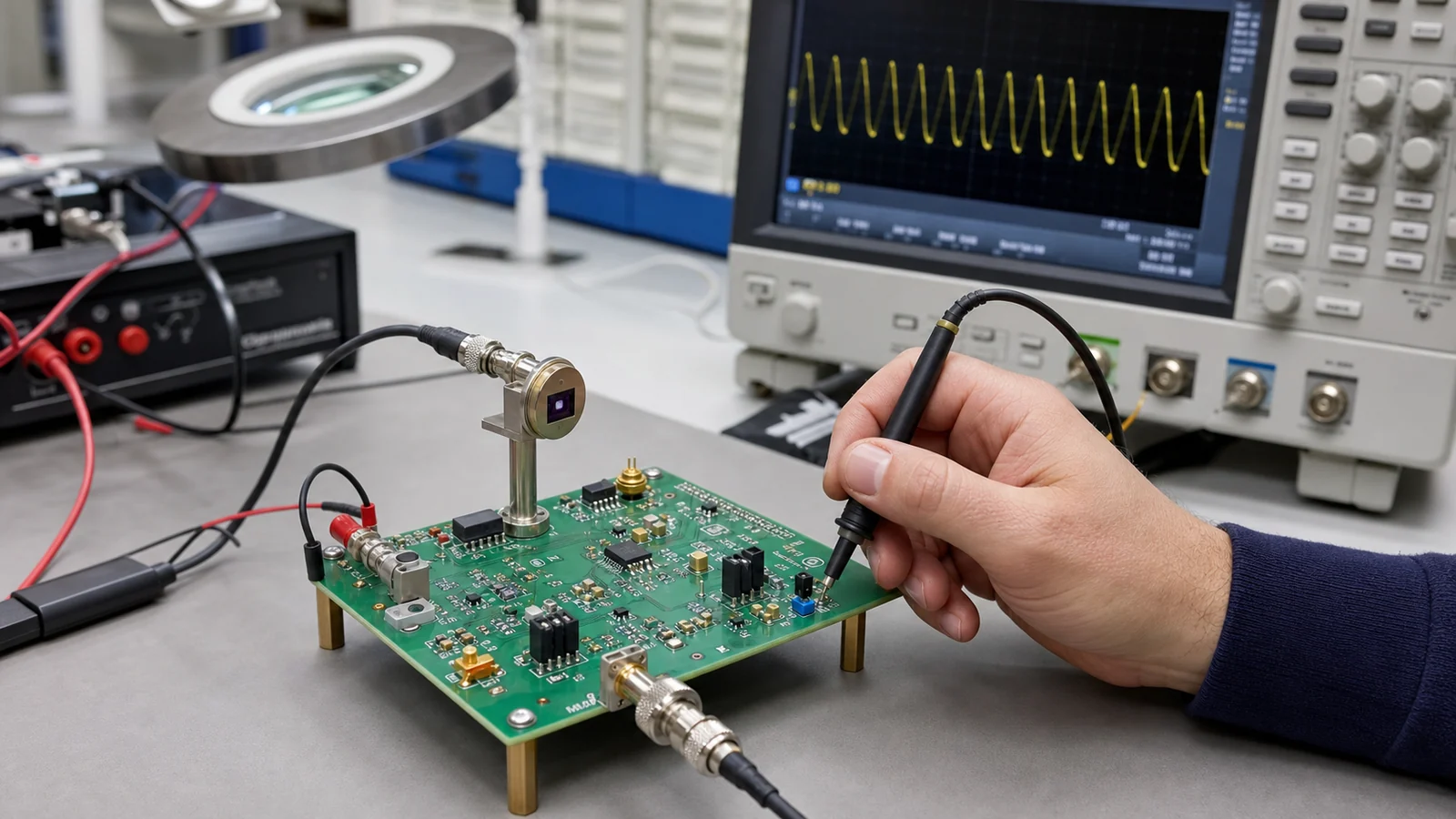
Once production starts, first-pass yield depends on a small number of controls that have to work together. A fast placement machine cannot rescue poor paste transfer. A perfect oven profile cannot correct wrong polarity. AOI cannot improve yield unless the findings loop back into print, placement, or design corrections.
1. Paste deposit control
Most SMT defects start as a volume or release problem. Paste age, stencil cleanliness, underside wipe frequency, support tooling, aperture reduction, and thermal-pad windowing all affect what lands on the pad. For dense boards, solder paste inspection is not just a quality gate; it is the fastest way to see whether the process is drifting before parts are placed.
2. Placement discipline
Placement reliability depends on feeder setup, nozzle condition, vision alignment, package library data, and component orientation. If an alternate package changes lead finish, package height, or body tolerance, the placement program may need a real update rather than a quick substitution note. Small errors here often appear later as skew, missing parts, polarity escapes, or intermittent test failures.
3. Thermal profile control
Reflow should match the assembled thermal mass, not an old recipe from a similar board. Heavy copper, large connectors, bottom-side parts, leadless packages, and dense ground planes can stretch the profile window. A safe profile has to wet the coldest joints without overheating sensitive parts or pushing the flux chemistry beyond its useful range.
4. Inspection feedback
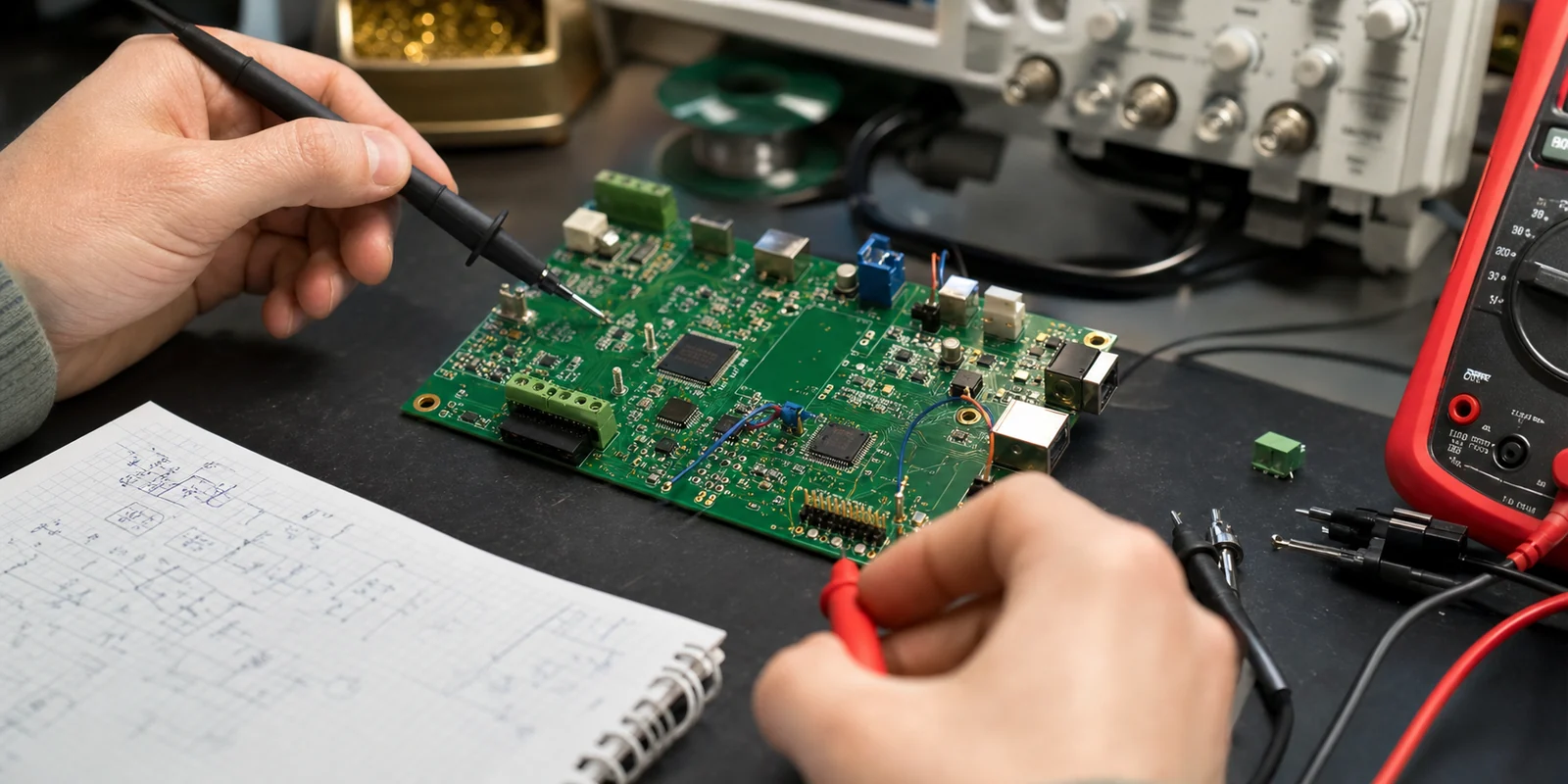
AOI, X-ray, ICT, and functional test are most useful when they change upstream behavior. If the same bridge repeats, the answer is usually not better operator attention; it is aperture design, pad balance, paste release, or component centering. If functional test fails late, the issue may be weak test-point access, firmware loading, connector seating, or traceability between the assembled lot and the programmed image.
Good BOM discipline and clear assembly process mapping belong in this same loop. The process is only stable when data, materials, machine setup, inspection, and test results all point back to the same build record.
Common Defects Usually Point Back to Earlier Decisions
Defects should be read as clues. A bridge, tombstone, or weak thermal-pad joint is not only a local soldering event; it often points to a design or preparation choice that was made earlier in the workflow.
- Tombstoning usually points to pad imbalance, uneven heating, mismatched terminations, or paste asymmetry.
- Fine-pitch bridging often indicates aperture strategy, paste release, stencil thickness, or insufficient print support rather than simply “too much solder.”
- Head-in-pillow defects can involve package warpage, oxidation, profile mismatch, or component handling before placement.
- Weak exposed-pad joints often trace back to thermal-pad aperture design, via-in-pad choices, voiding tolerance, or profile margin.
- Late functional-test escapes may reveal missing programming verification, limited test-point access, poor connector retention, or weak traceability.
The important habit is to push every repeated defect upstream until the team finds a controllable cause. Otherwise the same problem returns in the next lot with a slightly different symptom.
A Pilot Build Is Cheap Compared With Repeating the Wrong Process
Not every assembly needs a long qualification cycle, but many boards deserve a pilot lot before volume release. New package families, tight thermal-pad geometry, unfamiliar alternates, unusual panel constraints, dense connectors, and new functional-test coverage all add uncertainty. A pilot build gives engineering and manufacturing one controlled opportunity to measure that uncertainty before it becomes repeated scrap.
The goal of PCBA manufacturing is not merely to place components and create solder joints. It is to create a repeatable path from approved data to inspected, tested, traceable assemblies. A board that “can be assembled” is not the same as a board that can be built again next month after a supplier substitution, a paste change, or a fixture revision. The stronger the release package and feedback loop, the less drama the line has to absorb.
What is PCBA manufacturing?
PCBA manufacturing is the controlled process of turning bare printed circuit boards, approved component data, assembly instructions, inspection criteria, and test requirements into finished printed circuit board assemblies. It includes more than placement and soldering; it also includes data review, material readiness, process control, inspection feedback, and traceability.
How is PCBA manufacturing different from simple PCB assembly?
PCB assembly often refers to placing and soldering components onto a board. PCBA manufacturing is broader because it covers the release package, BOM control, approved alternates, stencil strategy, panel handling, reflow profile, AOI or X-ray review, functional test, and final production release.
Why do PCBA builds fail before the line even starts?
Many failures start before printing paste: incomplete manufacturer part numbers, mismatched package data, weak polarity notes, missing alternates, unclear centroid files, or panel and stencil assumptions that were never agreed with the assembler. The line then reveals the problem as delay, rework, or low first-pass yield.
What should an engineer send with a PCBA manufacturing package?
A useful package normally includes Gerbers or ODB++ data, centroid data, assembly drawings, an approved BOM with manufacturer part numbers, polarity notes, test expectations, firmware or programming instructions when needed, and clear rules for approved alternates and do-not-substitute parts.
When should you run a pilot build before volume production?
Run a pilot when the board uses new packages, fine-pitch parts, leadless thermal pads, unusual panel constraints, new sourcing substitutes, or a test strategy that has not been proven on the product. The pilot should confirm paste transfer, placement, reflow margin, inspection limits, and functional-test coverage before volume release.