A PCB assembly process flow chart is more than a training graphic. In real manufacturing, it acts as a shared map that keeps purchasing, SMT setup, soldering, inspection, and test aligned around the same build logic. When that map is vague, teams may still complete boards, but variation creeps in through feeder setup, paste printing, profile control, inspection criteria, and rework decisions. A clear workflow view makes it easier to reduce avoidable defects before they become schedule delays.
For engineers, sourcing teams, and buyers, the value of a process flow chart is practical. It shows where material data is needed, where yield risks are highest, and where handoff mistakes tend to happen. That matters whether you are building a quick prototype or preparing a repeat production run with a PCB assembly partner.

What a PCB Assembly Process Flow Chart Should Show
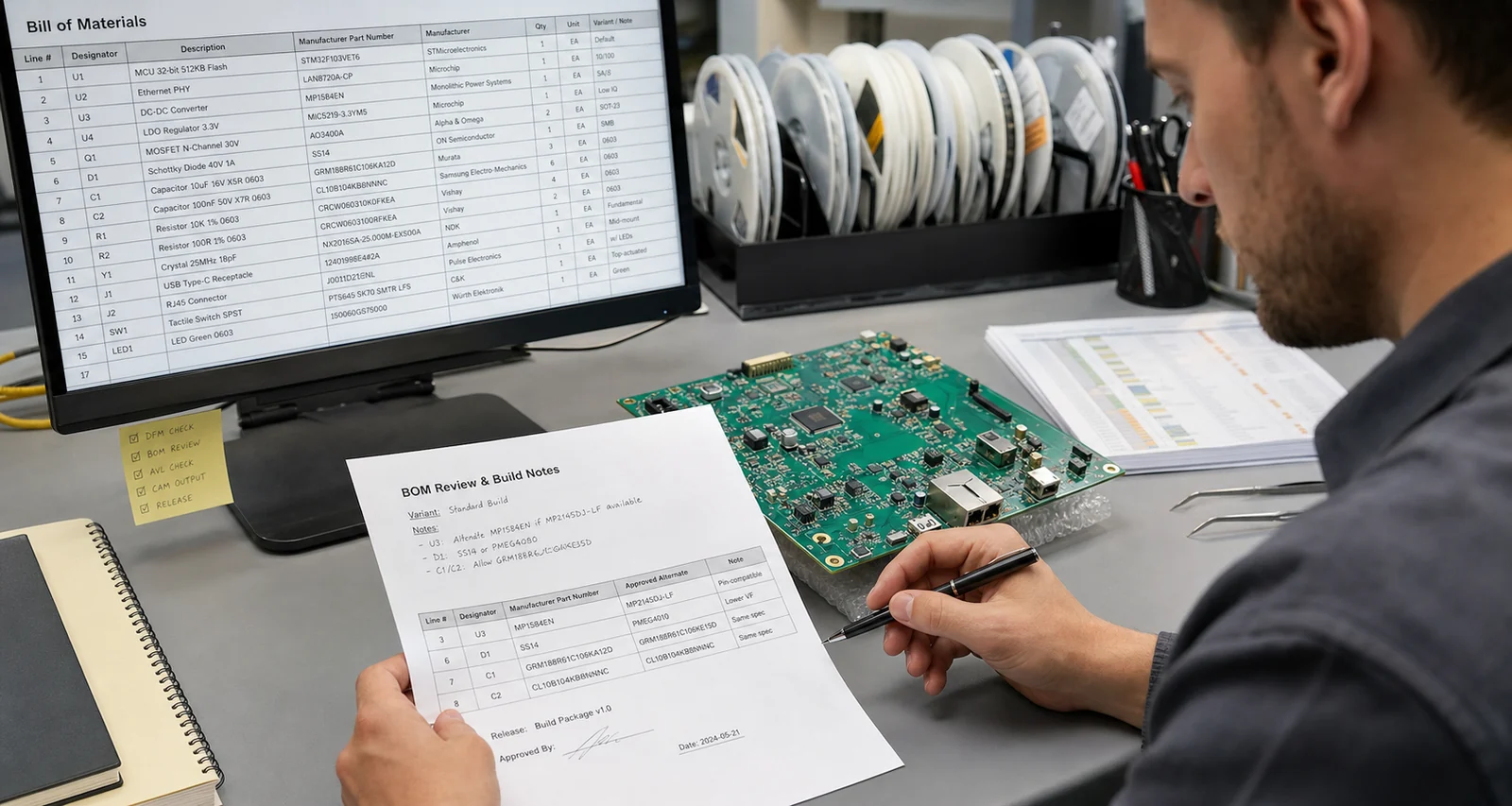
A useful chart should show the real order of manufacturing decisions, not only the machine sequence. In most builds, the workflow starts before a board touches the line. The release package must be checked for Gerbers, centroid data, BOM consistency, approved alternates, panel notes, stencil requirements, and special process instructions. If those inputs are incomplete, downstream process control becomes guesswork.
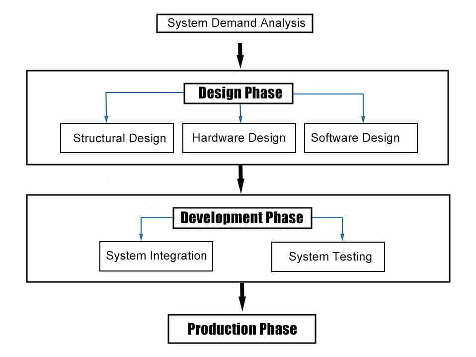
From there, the chart normally tracks six practical stages: incoming materials and data review, solder paste printing, component placement, reflow soldering, optical inspection, and functional verification. Depending on the product, manual insertion, selective soldering, conformal coating, or burn-in may also appear. The important point is that the chart should reflect the build you are actually buying, not a generic textbook line.
1. Incoming PCB, BOM, and Setup Review
The first stage is often underestimated because it does not look like manufacturing. Yet many yield problems begin here. The fabricator or assembler checks the bare boards, verifies the revision, confirms component availability, and compares the BOM against pick-and-place data. A mismatch between reference designators, package names, and approved substitutes can stall production or push operators into manual corrections.
This is also where design-for-manufacturing thinking matters. If the assembly drawing does not explain polarity, fiducials, panel rails, or special handling zones, the workflow becomes fragile. That is one reason many teams review manufacturability early with a structured DFM process instead of waiting for the first failed build.
2. Solder Paste Printing
Once setup is approved, the line usually begins with stencil printing. Solder paste volume is one of the strongest predictors of downstream quality, because every later stage depends on whether the correct amount of paste was placed on the correct pad. Too much paste can lead to bridging, slump, or solder beads. Too little can create opens, weak joints, or head-in-pillow style defects.
A flow chart should not treat printing as a simple one-box action. It should imply stencil alignment, paste condition, wipe frequency, and inspection discipline. On dense boards, even small aperture or support issues can create systematic defects that no placement machine can fix later.
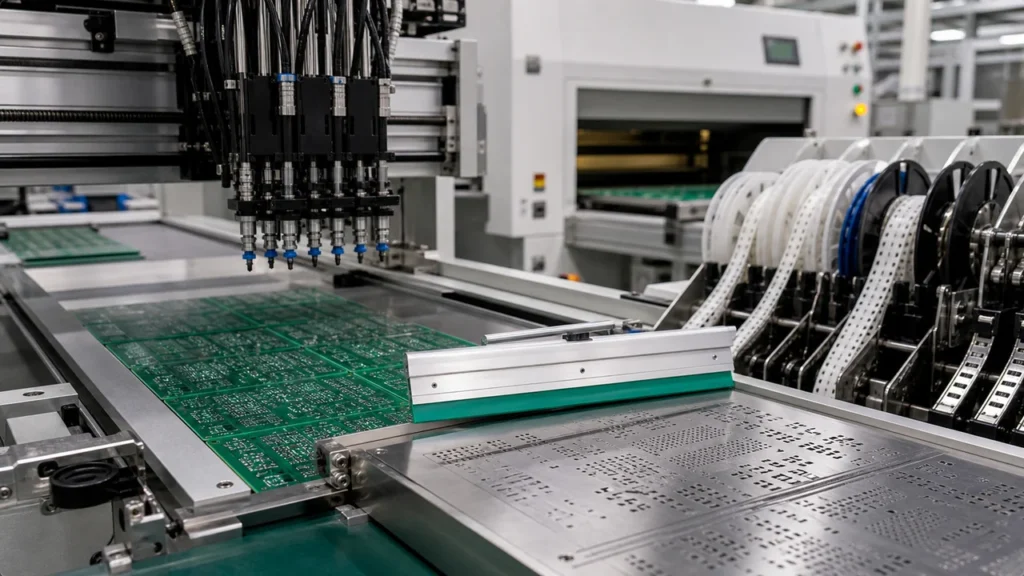
3. SMT Placement
After printing, components are placed onto the pasted pads. In the chart, this step looks straightforward, but it depends on feeder loading, package libraries, nozzle selection, vision alignment, and placement force. A modern line can place quickly, yet repeated errors still come from wrong part reels, rotated polar parts, poor fiducials, and mismatched land pattern assumptions.
This is why the best flow charts connect placement to the setup review stage. If a package in the BOM does not match the board footprint, the process problem did not begin at the machine. It began in data control. For mixed-technology boards, the chart may also split between SMT placement and later manual insertion to show where the process branches and rejoins.
4. Reflow Soldering
Reflow is where the printed paste becomes the final solder joint, so the thermal profile deserves explicit attention in any PCB assembly process flow chart. Preheat, soak, time above liquidus, peak temperature, and cooling all affect wetting, voiding, tombstoning, and component stress. A chart that ignores thermal control makes the process look simpler than it is.
For boards with high copper imbalance, large thermal masses, or heat-sensitive parts, process engineers often validate profiles using thermocouples on the actual assembly. That is one reason line selection matters when you compare suppliers. If you need more context on thermal equipment, the broader discussion in PCB oven processing helps explain why oven capability is part of assembly quality, not an afterthought.
5. AOI and Visual Inspection
After reflow, automated optical inspection usually checks for presence, polarity, tombstones, offset parts, bridging, and other visible anomalies. In practice, AOI is not magic. It works best when the assembly data, lighting strategy, component library, and pass-fail criteria have been tuned to the product. Otherwise, teams waste time chasing false calls or, worse, miss repeated defects because the inspection recipe was built too loosely.
A strong flow chart therefore treats AOI as a decision stage, not a decorative box. The path after AOI should be clear: pass to test, route to review, or send to controlled rework. That visibility is important for buyers as well, because it reveals whether the supplier operates a disciplined process or simply reacts to problems after shipment risk increases.
6. Functional Test and Release
Electrical verification is the last major stage in a standard PCB assembly process flow chart. Depending on the product, that may mean continuity checks, in-circuit measurements, power-on bring-up, firmware loading, boundary conditions, or fixture-based functional test. The key is that the board should not be considered production-ready just because it looks clean after AOI.
For higher-risk products, teams often add serial traceability, failure logging, and repair feedback into this final stage. That closes the loop between test results and earlier process steps. If a recurring defect points back to stencil deposition or thermal imbalance, the flow chart becomes a tool for process correction rather than a static illustration.
Where Flow Charts Help When Choosing a Supplier
Many companies ask for a quote before asking how the line is actually run. That is backwards. A process flow chart helps you compare suppliers on more than unit price. You can ask whether incoming data is reviewed by engineering, whether stencil inspection is routine, whether AOI is standard for your board class, and what kind of test evidence is retained. Those questions often tell you more than a sales claim about fast turnaround.
It is also useful when discussing prototype versus repeat production. Some suppliers are excellent at fast pilot builds but less structured on documentation and repeatability. Others are strong on volume control. If you are still evaluating vendors, reviewing examples such as a PCB assembly company comparison can help frame the right process questions before you release a build.
Common Mistakes in a Simplified Workflow
The most common mistake is treating the chart as a machine list instead of a control plan. Another is forcing all boards into the same sequence even when hand insertion, selective soldering, cleaning, or coating changes the real routing. A third is hiding rework and inspection decisions, which makes post-reflow quality look binary when it rarely is.
Good documentation does not need to be complicated, but it must show where defects can be prevented, detected, and fed back into the process. That is what turns a PCB assembly process flow chart into a practical manufacturing document instead of a presentation slide.
Bottom Line
A well-built PCB assembly process flow chart gives engineering and procurement teams a common view of how boards move from released data to verified hardware. It clarifies where quality is created, where risk concentrates, and what questions to ask before the first panel enters the line. If the chart reflects real setup review, printing control, placement discipline, thermal validation, inspection logic, and test closure, it becomes a useful production tool rather than a generic graphic.
What is the main purpose of a PCB assembly process flow chart?
Its main purpose is to show the real build sequence and the control points between steps, so engineering, purchasing, and manufacturing teams understand how the board moves from released data to verified assembly.
Does every PCB assembly process follow the same exact chart?
No. The core stages are often similar, but mixed-technology boards, selective soldering, conformal coating, burn-in, or special test requirements can change the routing and add decision points.
Why is AOI shown separately from reflow in the workflow?
Because reflow creates the solder joints, while AOI evaluates whether the visible result meets process expectations. Keeping them separate makes inspection and defect routing explicit.
Can a process flow chart help when choosing a PCB assembly supplier?
Yes. It helps you ask better questions about setup review, paste control, profile validation, inspection coverage, test evidence, and how the supplier manages repeatability beyond the quoted price.