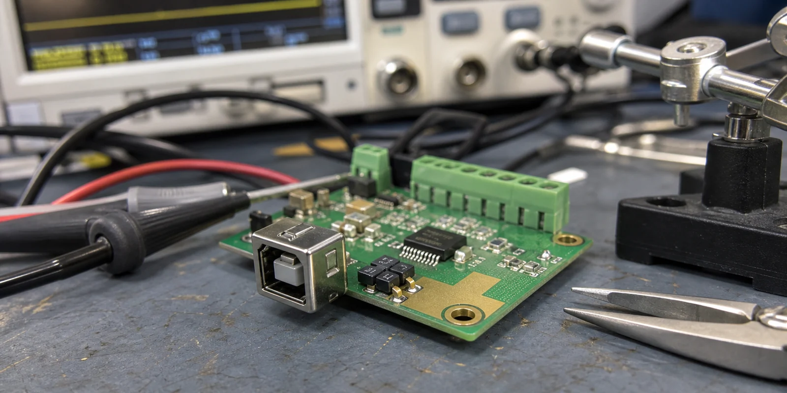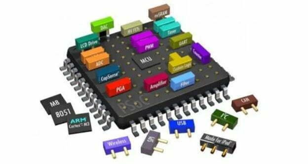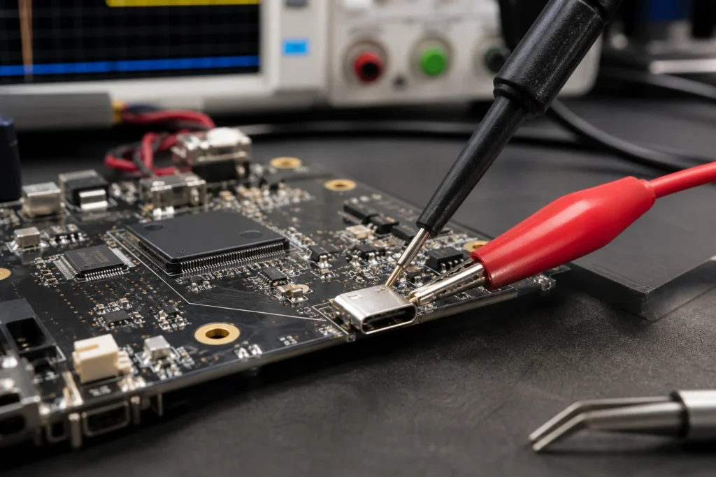
A USB wiring schematic is easy to oversimplify because most search results show a cable color chart or a four-wire diagram with almost no board context. That is enough to identify VBUS, D+, D-, and GND on a bench cable, but it is not enough to design or debug a real USB port on a PCB. The moment you move from a loose cable to a connector on an assembled board, details such as connector role, shield termination, ESD placement, CC or ID behavior, and power switching start deciding whether the port enumerates cleanly or fails in ways that are expensive to trace.
This guide focuses on the PCB-level checks that make a USB wiring schematic usable in practice. It keeps the common USB 2.0 signal set as the baseline, then shows where Micro-USB, USB-C, and board debug work change the wiring decisions.
Start by identifying which USB interface the schematic is really describing
The first job is to separate a cable diagram from a board schematic. A basic USB 2.0 cable usually gives you VBUS, D-, D+, and GND. A board schematic may add shield connections, ESD protection, a polyfuse or load switch on VBUS, common-mode filtering, USB-C configuration channel resistors, or a Micro-USB ID pin. If the drawing does not tell you which connector family and device role it belongs to, the “USB wiring schematic” is incomplete before routing even begins.
For a practical ReversePCB workflow, label three things immediately: connector type, data speed target, and role. A USB-C receptacle used only for USB 2.0 device power and data does not need the same schematic detail as a host-capable port, a charging-only port, or a superspeed design. Teams often copy a generic connector symbol, wire the visible pins, and assume the rest can be handled in layout. That shortcut is where wrong CC resistors, floating shields, or missing overcurrent protection start.
What the core USB 2.0 wiring still has to show on a PCB
A usable USB 2.0 schematic must show more than four named nets. At minimum, it should make the path of power, data, return current, and protection obvious enough that another engineer can review it without guessing design intent.
For a device-side USB 2.0 port, the baseline checks are straightforward:
Power path
VBUS should not disappear into the board without a reasoned path. If the port powers the board, show the fuse, current limit switch, transient protection, or input power management that stands between the connector and the downstream rail. If the board is self-powered, show clearly whether VBUS is only used for cable-detect or attach-detect behavior.
Data pair
D+ and D- should stay named as a pair and should route to the USB transceiver or MCU pins without unexplained test-point branches, jumper options, or series parts scattered across the sheet. Short stubs added for debug clips or fixture access can be enough to create marginal full-speed or high-speed behavior when the board already has connector and cable loss.
Ground and shield
Ground must be explicit, and shield handling must not be left to layout interpretation. Some designs bond shield directly to board ground near the connector. Others use a chassis strategy, resistor-capacitor network, or bead based on enclosure and EMI goals. The important point is that the schematic must show the intended strategy. Leaving shield floating “for later” often turns into inconsistent assembly revisions and noise-sensitive field behavior.
Where USB connector families change the wiring rules
The same net names do not mean the same review checklist across Type-A, Type-B, Micro-USB, and USB-C. This is where many generic diagrams fail a real design review.
Micro-USB adds the ID pin question. If the product uses USB OTG or accessory detection, the schematic has to show how ID is treated. If it is a device-only product, leaving the pin unused may be correct, but the decision should still be documented so test and repair teams do not assume a missing connection is a fault.
USB-C changes the problem more substantially. A USB-C receptacle that only carries USB 2.0 still needs correct CC handling to advertise sink, source, or dual-role behavior. If the schematic simply ties D+ and D- to the expected USB 2.0 pair but ignores the CC pins, the port may never attach correctly even though the board “looks wired.” In production, this often shows up as a board that powers from one cable orientation or one charger family but not another.
For beginner teams, this is the same reason a generic pinout definition is only the starting point. A connector pinout tells you what can connect. The schematic must show how your board is supposed to behave after those pins are connected.
Common USB wiring schematic mistakes that survive review too easily
The most common failures are not exotic. They survive because the schematic looks familiar enough that reviewers stop asking the last practical question.
One frequent mistake is treating D+ and D- as ordinary digital lines. That leads to unnecessary vias, mismatched branch points, or long detours to ESD arrays that should have been placed close to the connector entry. Another is placing ESD protection symbolically on the sheet but not in a position that can actually clamp the transient before it reaches the transceiver pins. On a finished board, the difference between “on the same net” and “electrically first in line” matters.
A second class of mistakes comes from power assumptions. Designers sometimes feed VBUS directly into a local regulator without checking inrush, hot-plug stress, back-power paths, or host-current limits. If a board can also be powered externally, the schematic should make reverse-current blocking unambiguous. Otherwise, technicians may see a “USB problem” that is really a power OR-ing mistake.
A third mistake is under-documenting shield and return strategy. This becomes visible during EMC troubleshooting, ESD testing, or intermittent laptop-connection complaints. If your enclosure, mounting hardware, or cable assembly creates multiple return paths, the schematic should give manufacturing and compliance reviewers a single intended connection strategy instead of forcing them to infer it from copper alone.
The same review discipline used in a TVS suppressor diode selection also applies here: protection only works as intended when the protected path, return path, and clamp placement are explicit.
What a PCB-ready USB wiring schematic should include before layout starts
A PCB-ready USB wiring schematic should let layout, test, and debugging teams answer practical questions without opening a second document. If it cannot do that, it is still a concept diagram rather than a release-ready schematic.
At a minimum, show connector reference designator, exact pin mapping, the transceiver endpoint, the VBUS conditioning path, ESD parts, and any role-detect components. If the board uses USB-C, identify CC pull-up or pull-down values and which controller or policy device owns them. If the board uses a common-mode choke or series resistors, place them in the schematic in the same order the signal sees them from the connector inward.
Test access also matters. If the product may need bring-up, fixture testing, or depot repair, decide in the schematic where USB-related measurements can be made without cutting solder mask or lifting fine-pitch connector pins. A tiny board with no accessible VBUS test point and no clean ground reference can turn a one-minute continuity check into a destructive rework attempt.
For low-volume prototypes, adding a deliberate test pad pair for D+ and D- near the transceiver is sometimes worth the routing cost if the connector is mechanically difficult to probe. For higher-speed designs, you still have to judge whether that access point creates a stub you cannot afford. The schematic should at least show that the tradeoff was considered.
How to debug a USB port when the schematic looks correct but the board still fails
A failed USB port often looks like a firmware problem at first, but the fastest diagnosis usually starts with the wiring path. Confirm connector orientation, continuity from connector pins to the intended device pins, VBUS presence under load, and whether shield and ground reference points are behaving as designed. If the product uses USB-C, verify CC behavior before chasing data-pair faults; a bad attach state can make the data path look dead even when D+ and D- are routed correctly.
Then check whether the board is failing the same way across different cable families. A board that works with a short known-good cable but not with a longer or stiffer cable may have marginal protection placement, weak connector solder joints, or too much routing discontinuity. A board that powers but never enumerates may point to swapped D+ and D-, a missing pull-up, wrong USB role handling, or a damaged transceiver.
Repair reality matters here. Replacing a USB connector without checking pad adhesion, anchor tab integrity, and nearby ESD parts is a common trap. On boards that have seen repeated cable stress, the visible connector damage is sometimes only the last failure. Cracked solder joints, torn anchor pads, or shield-ground fractures can leave the new connector behaving exactly like the old one.

When a simple USB wiring schematic should become a design checklist instead
Some USB topics are too broad to solve with one neat diagram. If the board has dual-role behavior, power negotiation, ESD compliance risk, or mixed internal and external power paths, the schematic should be paired with a short design checklist. That checklist can cover cable orientation behavior, CC network verification, protection placement review, inrush and back-power checks, and the exact bench tests needed before release.
This is especially useful in contract manufacturing or mixed-team environments. A schematic that is technically correct but poorly annotated can still lose intent during ECO review, test-fixture creation, or service documentation. A short release checklist costs far less than a field return caused by one misread connector option or one omitted shield bond.
A USB wiring schematic is only useful when it matches the real board behavior
The safest way to use a USB wiring schematic is to treat it as a board-behavior document, not just a pin map. Once connector type, role, VBUS handling, protection order, and debug access are explicit, the drawing becomes genuinely useful for design review and troubleshooting. If those items are missing, the schematic may still help you identify wires, but it will not reliably prevent the PCB-level mistakes that cause failed enumeration, damaged ports, or expensive rework.
FAQ
Is a USB wiring schematic the same as a USB pinout?
A pinout only tells you which signal belongs to which connector pin. A practical USB wiring schematic also shows how those pins connect into the board, including VBUS protection, shield handling, CC or ID behavior, and the data-pair path to the transceiver.
What is the most common USB schematic mistake on a PCB?
The most common mistake is using a generic connector diagram without showing the real board behavior. That usually means missing CC handling on USB-C, weak VBUS protection, poor shield-ground definition, or D plus and D minus protection parts placed too far from the connector entry.
Can I use one USB wiring schematic for Type-A, Micro-USB, and USB-C?
Not safely. The core USB 2.0 data pair may look similar, but Micro-USB can involve an ID pin and USB-C requires correct CC behavior even when you only use USB 2.0 data. Reusing one generic schematic across connector families often creates attach or power-path errors.
Why does a board work on one cable but fail on another if the USB wiring looks correct?
That usually points to a marginal board implementation rather than a purely logical wiring error. Common causes include weak connector joints, poor ESD placement, excessive pair discontinuity, unstable shield return behavior, or a USB-C attach network that only behaves correctly with some chargers or hosts.