The Ultimate Guide to PCB Vias
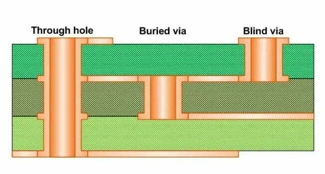
Learn via types: through-hole, blind, buried, and vias-in-pad. Tips for spacing, drilling, and reliability in multi-layer PCBs. Essential for advanced layouts. Guide inside!
Schematic & Gerber restoration
MCU/CPLD code restore access & backup
1:1 exact hardware replication
BLE & Classic BT wireless solutions
Precision PID & thermal management
High-efficiency motor drive control
Industrial RS485/RTU communication
Custom STM32/ESP32 firmware & HW
Calculate the PCB trace width based on temperature rise, current, and copper thickness (IPC-2152).
PCB design and manufacturing are critical steps in building electronic products. Our guides and tutorials cover everything from schematic design and layout to fabrication and assembly. Learn best practices for designing efficient, high-quality PCBs and gain insights into the entire manufacturing process, ensuring your designs are optimized for performance and cost.

Learn via types: through-hole, blind, buried, and vias-in-pad. Tips for spacing, drilling, and reliability in multi-layer PCBs. Essential for advanced layouts. Guide inside!

1. Develop and design cooperation methods:Software design: MCU software development and design, according to customer requirements, write the required functional software; or rewrite the software part according to the customer’s actual hardware.Schematic design: Design circuit schematics according to customer requirements.PCB

This circuit is based on the PCB design of the capacitance test circuit of the PlCl6LF874 microcontroller. The specific contents are as follows. How the Capacitance Measurement Module WorksThe overall design principle block diagram of the capacitance measurement module is

BGA is a commonly used component on PCB, usually CPU, NORTH BRIDGE, SOUTH BRIDGE, AGP CHIP, CARD BUS CHIP, etc. They are mostly packaged in bga type. In short, 80% of high-frequency signals and special signals will be pulled by

We have advanced equipment to support rapid PCB prototyping. Depending on the situation, the entire production process takes about one to three weeks. The prototype is first tested in the laboratory, and we will send the test report to the

VR Gaming Technology Virtual Reality (VR) gaming technology is a rapidly advancing field that enables players to immerse themselves in a computer-generated 3D environment. With advances in hardware and software, players can interact with and explore a virtual world in

Interactive Guide to PCB Prototype Costs PCB Cost Guide Overview Cost Drivers Strategies Calculator Case Studies FAQ OverviewCost DriversStrategiesCalculatorCase StudiesFAQ Decoding PCB Prototype Costs Welcome to the Interactive Guide to PCB Prototype Costs. This application is designed to help you

What is 6-Layer PCB Manufacturing? 6-layer PCB manufacturing is the mass-production of PCBs with a minimum of six layers. In a 6-layer PCB, the top and bottom layers are usually made of laminated material which is then covered with a

Through-hole PCB design: components, soldering, and pros/cons vs SMT. Best practices, tools, and project examples. Essential for beginners and engineers!

PCB designers need to understand PCB trace basics to create high-performance printed circuit boards. From basic definitions to the types of traces, this article covers all the fundamentals you need. Working with printed circuit board (PCB) design software can be