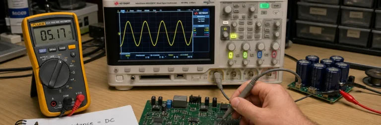
Impedance Versus Resistance in PCB Work Is Really a Question of Frequency
Resistance explains static loss and voltage drop, but impedance decides how PCB traces, capacitors, drivers, and interconnects behave once frequency and edge rate matter.

Resistance explains static loss and voltage drop, but impedance decides how PCB traces, capacitors, drivers, and interconnects behave once frequency and edge rate matter.
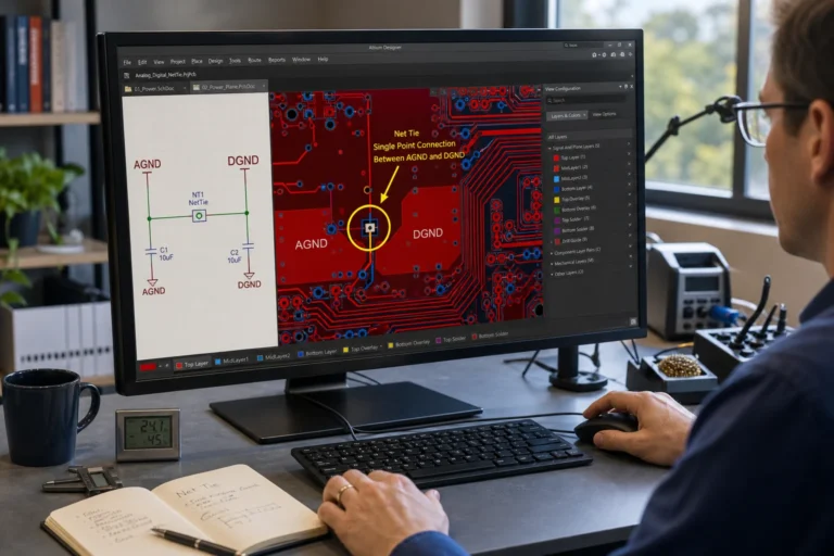
An Altium net tie is useful when two nets must meet at one intentional location without losing their names, rules, or review visibility everywhere else.
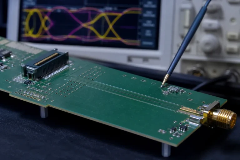
Impedance mismatch on a PCB usually appears first at the launch, via field, connector, or return-path break where the signal stops seeing the geometry you modeled.
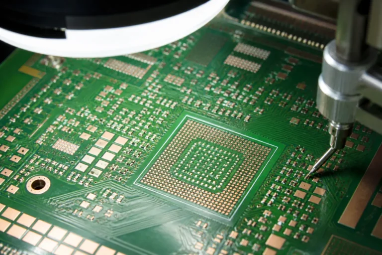
PCB solder mask thickness matters when it starts changing pad definition, inspection clarity, outer-layer impedance assumptions, and the assembly window around dense features.
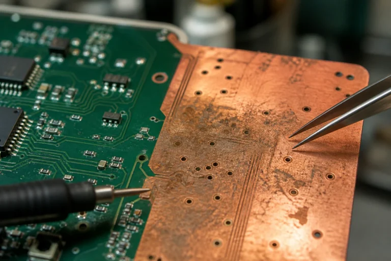
A PCB without solder mask can oxidize, stain, bridge during assembly, and become harder to inspect or rework unless the exposed copper area is intentional and tightly controlled.
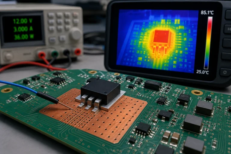
Thermal impedance is only useful when you know whether the datasheet number describes a package test board, a case path, a board path, or a short pulse event in your real design.
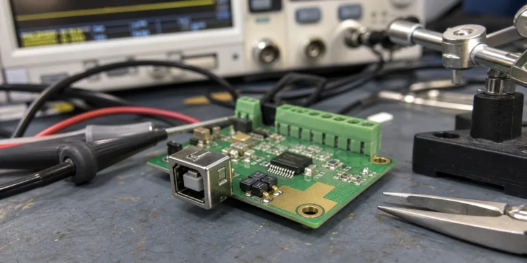
A TVS suppressor diode only protects a PCB when standoff voltage, clamp behavior, surge energy, and layout placement match the actual threat at the connector.
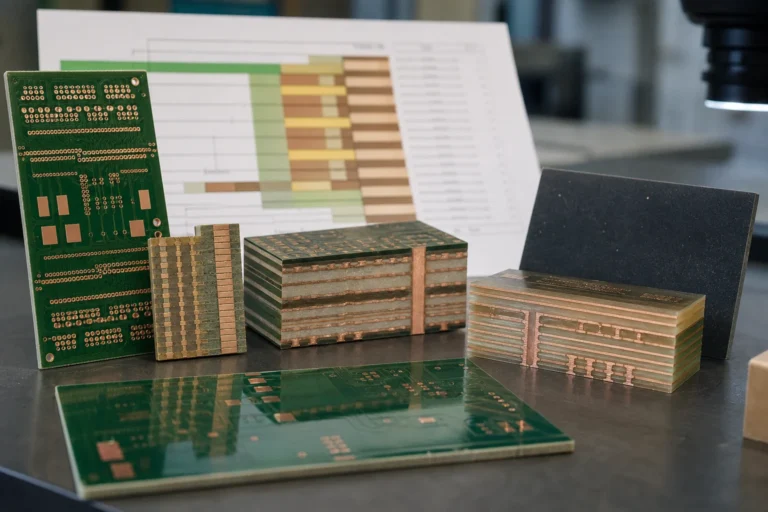
Standard 2-, 4-, 6-, and 8-layer PCB stackups only work when return paths, impedance, copper balance, and fabrication assumptions still match the real design.
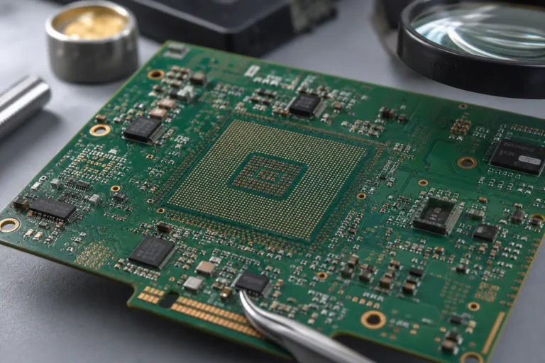
Via in pad can solve dense BGA and QFN escape problems, but only when fill, cap, planarity, paste behavior, and inspection risk are reviewed before release.
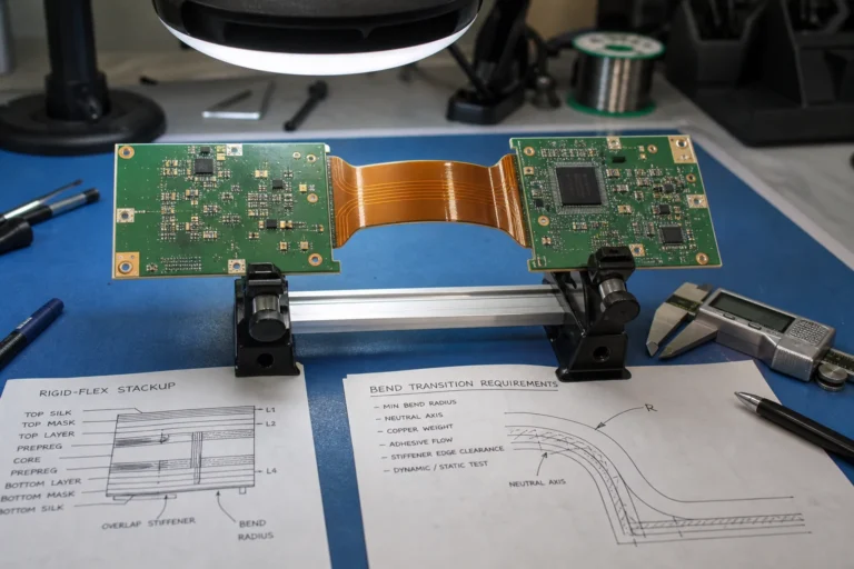
A rigid-flex PCB stackup is not just a layer list. It sets bend reliability, copper strain, stiffener transitions, impedance behavior, and assembly risk long before fabrication starts.