Solder mask thickness sounds like a small fabrication detail until it starts changing paste release, pad exposure, optical inspection, or the last few ohms of an impedance target. On a simple two-layer board, the effect may be modest. On fine-pitch assembly, exposed-pad power parts, or high-speed traces close to the outer layer, mask thickness becomes part of the process window rather than a line item in a fab note.
This guide explains what PCB engineers should really check when discussing solder mask thickness with a board house. The useful question is not just how many microns the mask measures. It is whether that thickness still works with your pad geometry, finish, stencil, inspection method, and electrical assumptions.
What Solder Mask Thickness Actually Changes on a Real PCB
Solder mask thickness affects more than board appearance. It changes how clearly pad edges stay defined, how much mechanical protection the copper sees, how close a mask dam can survive between adjacent pads, and whether outer-layer impedance assumptions still line up with production reality. It also changes how forgiving the board is during assembly and rework.
That matters because a nominal thickness on a data sheet is not the whole story. Mask can vary over copper steps, near vias, around sharp pad corners, and between board houses using different liquid photoimageable materials or cure profiles. If the takeaway is only “thicker is better protection,” the engineer still does not know whether the process will hold fine dams, survive rework, or stay consistent over the copper topography that matters on the real board.
Start with Pad Geometry and Mask Dams Before You Think About Protection
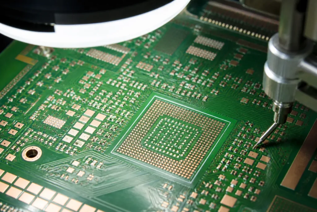
The first practical check is simple: can the mask still resolve the spaces your footprint requires? Fine-pitch QFN, small-pitch connectors, and dense LED or RF layouts are often limited by mask registration and dam survival before they are limited by copper etching. If the mask bridge collapses, solder bridging risk rises fast and AOI images become harder to trust.
This is where thickness and resolution interact. A board house may quote an average cured mask thickness, but the more urgent question is whether that process can hold clean openings and stable slivers at your design pitch. For assembly yield, a slightly thinner but better-controlled mask process can beat a thicker coating that prints poorly around tight pads.
Why Assembly Results Change When the Mask Is Too Thin or Too Heavy
If the mask is too thin in exposed areas, copper protection and chemical resistance suffer, especially around rework-prone regions or boards that see more than one thermal cycle. If it is too heavy around tight pads, it can distort the opening geometry, trap flux, or create uneven solder behavior near the pad edge. Neither failure mode is dramatic on a bare board review. Both show up later in print quality, fillet shape, and cleaning behavior.
Assemblers feel this first on boards with small passive arrays, mask-defined pads, and exposed thermal pads. A heavy mask edge can slightly change how paste volume releases at the boundary. A weak mask process can chip during depanelization or rework and contaminate a repair area that was already hard to service. Those are not textbook effects, but they are real production costs.
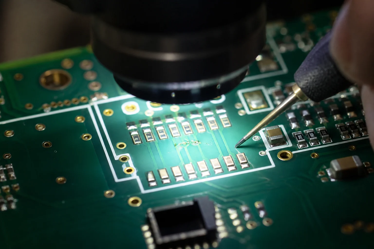
Solder Mask Thickness Can Also Shift Outer-Layer Impedance Assumptions
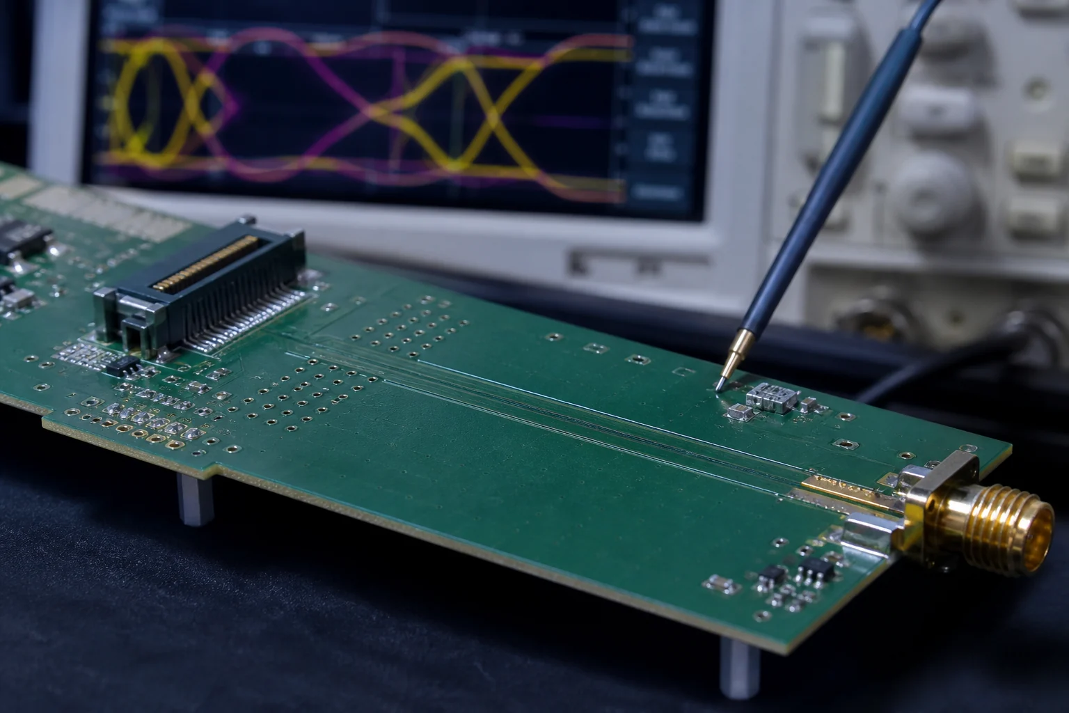
On outer-layer controlled-impedance traces, solder mask is part of the electromagnetic environment. The effect is not always dominant, but it is real enough that serious impedance work should not ignore it. ReversePCB’s own PCB impedance calculator includes solder mask thickness because it changes the effective dielectric environment above the conductor.
That does not mean every board needs a custom mask-thickness study. It means the mask note should stay consistent with the stackup, surface finish, and coupon strategy when the target tolerance is tight. Teams sometimes sign off an impedance model with one outer-layer assumption and then accept a different mask build in fabrication because the copper still looks fine on the drawing. The coupon may pass differently from the signal path you thought you designed.
How to Discuss Thickness with the Fabricator Without Getting a Vague Answer
Do not ask only for a “standard solder mask thickness.” Ask how the supplier defines the measurement, where it is measured, what variation is typical over copper features, and whether your design includes any mask-defined pads, tight dams, controlled-impedance outer layers, or rework-sensitive areas. That is the difference between a quote answer and an engineering answer.
If the board is sensitive, request alignment between the fabrication note, the impedance model, and the assembly assumptions. For example, if you expect tight impedance tolerance and also have fine-pitch pads near high-speed escape routing, the fab note should not leave mask choice completely open. The supplier may still propose an equivalent process, but the risk should be discussed before the first lot is built.
When Thickness Matters Less Than Registration and Process Control
Many PCB teams ask the wrong question because thickness is easy to compare on paper. In practice, poor registration, weak cure control, or inconsistent opening quality often cause more trouble than the nominal cured thickness. A stable process with clean openings and repeatable alignment beats a thicker mask that looks protective in a table but behaves poorly around dense pads and vias.
This is especially true for prototype-to-production transitions. Early boards may pass because the operator manually cleans up defects or because the build quantity is small. Once volumes rise, the weak point moves from visual appearance to repeatability. That is where mask process control, not just target thickness, determines yield.
For a broader refresher on how mask functions beyond color and cosmetics, the existing About Solder Mask article is a good background read. If the question is how thickness interacts with the finished board build, standard PCB board thickness is also useful context because thickness decisions rarely live in isolation.
A Practical Review Checklist for Solder Mask Thickness
- Confirm whether the design depends on fine mask dams, mask-defined pads, or tight registration around dense pads.
- Check whether outer-layer impedance assumptions include solder mask thickness and dielectric effect.
- Review rework-sensitive or exposed-pad zones where chipped or uneven mask will raise repair cost.
- Ask the fabricator how thickness is measured and what variation is typical over copper features.
- Align mask assumptions with stencil design, AOI visibility, and the assembly process rather than treating mask as a standalone fab item.
If a board does not have dense assembly, tight impedance tolerance, or delicate repair zones, standard mask thickness may be perfectly adequate. If it does, the right question is not whether the mask is “thick enough.” It is whether the process still supports the board you are actually trying to build.
FAQ
Does solder mask thickness affect controlled impedance?
Yes, on outer-layer traces it can. The mask changes the dielectric environment above the conductor, so tight impedance work should keep mask assumptions aligned with the stackup and fabrication process.
Is thicker solder mask always better for protection?
No. More thickness does not automatically improve yield. If the process loses opening quality, registration accuracy, or clean mask dams around dense pads, a thicker coating can create new assembly problems.
What should I ask a PCB fabricator about solder mask thickness?
Ask how the thickness is defined and measured, how much variation is typical over copper features, and whether the process can still support your pad spacing, mask dams, impedance assumptions, and rework expectations.
When does solder mask thickness matter most?
It matters most on boards with fine-pitch assembly, mask-defined pads, outer-layer controlled impedance, exposed thermal pads, or repair-sensitive areas where weak mask control will increase yield loss or rework cost.