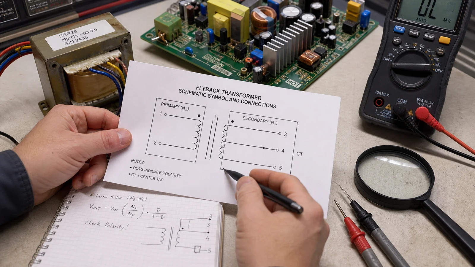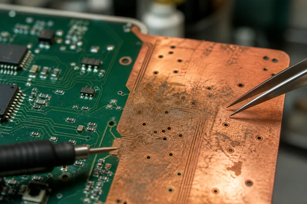
A PCB without solder mask rarely fails because someone forgot what solder mask does in theory. It fails because exposed copper starts interacting with storage air, handling residue, solder paste spread, cleaning chemistry, and field contamination long before the board reaches a dramatic visible defect. By the time the copper looks dark or uneven, the real damage may already be showing up as weak solder wetting, leakage paths, cosmetic rejection, or rework that takes longer than the board budget allowed.
This article looks at the practical engineering question behind the awkward keyword copper oxydation no solder mask pcb: what really happens when copper stays exposed on a board, when that choice is intentional, and how to keep it from turning into an avoidable reliability problem.
Exposed copper on a PCB creates more than an oxidation problem
Oxidation is the obvious concern because bare copper darkens quickly once it is no longer protected by finish, mask coverage, or controlled packaging. But the bigger engineering problem is that exposed copper becomes sensitive to everything around it. Finger oils, humid storage, ionic residue, aggressive cleaning, and loosely controlled rework all have easier access to the conductor surface when there is no mask barrier to isolate adjacent areas.
That changes multiple failure modes at once. Solderability can drift because the copper surface no longer wets consistently. Fine-pitch spacing becomes less forgiving because solder mask is not there to resist paste spread or stray hand-solder bridges. Inspection also gets harder because discoloration, light staining, and harmless cosmetic variation can sit next to genuine corrosion or contamination, and technicians end up debating whether the board is merely ugly or already unreliable.
A standard solder mask does not exist only to make a board look finished. It also helps control bridging, defines exposed metal boundaries, limits accidental shorting during handling, and gives the factory a more stable surface condition between fabrication, assembly, and service.
Why exposed copper ages badly in storage and on the line
A no-mask area does not wait for field use to become risky. Problems often start between fabrication and assembly. If copper is exposed broadly rather than only where it is supposed to be soldered or contacted, the board becomes much more dependent on packaging discipline, humidity control, finish choice, and how long it sits before the next process step.
On a quick-turn prototype, a bare-copper area may still look acceptable when it moves from fab to bench within days. That same design can behave very differently in a production environment where boards are panelized, depanelized, touched by operators, staged in trays, or held in stock before assembly. A pad that still solders well on day three can become inconsistent after a longer delay, especially if the surface finish was chosen for cost instead of shelf stability.
Once assembly begins, exposed copper also makes process variation more visible. Paste slumping onto unmasked copper can create solder beads or hidden bridges. Selective soldering can wick farther than expected. Rework operators have fewer visual boundaries when dragging solder away from a joint. None of those issues need dramatic corrosion to become expensive.
When leaving copper exposed is intentional and still acceptable
Not every exposed copper area means the PCB was designed badly. Many boards deliberately leave metal open where the function requires contact, heat transfer, tuning access, or a defined finish surface. The difference is that these openings are intentional, limited, and supported by process rules.
Common examples include test pads, edge contacts, thermal pads, shielding contact zones, exposed high-current copper used with mechanical fastening, or RF structures where extra mask thickness would affect performance. In those cases, the exposed area is usually paired with a surface finish, dimensional control, contamination limits, and a clear reason for why mask coverage would create a worse problem.
The practical question is not whether any copper can ever be exposed. The question is whether the opening has a specific electrical, mechanical, or thermal job. If the answer is vague, such as “it should be fine without mask” or “the copper is only there for convenience,” the design is already drifting into avoidable risk.
How oxidation changes solderability, leakage, and repair decisions
Oxidized copper does not always fail in one obvious way. Sometimes the board still assembles, but wetting is slower and joints become more operator-dependent. Sometimes the first build passes, but later rework becomes harder because the exposed copper around the joint has seen more heat cycles and more contamination. On fine-pitch or high-impedance circuits, the bigger concern may not be soldering at all. Moisture and residue on exposed copper can make leakage, noise pickup, or intermittent behavior harder to reproduce.
This matters most where engineers expect the board to be reworked or measured in the field. Exposed copper invites scraping, probing, and improvised soldering because it looks accessible. That often accelerates damage. A technician may tin a bare area to rescue a broken trace or attach a wire, only to discover that the surrounding copper lifts more easily than expected because the area was never designed for repeated thermal abuse.
Repair reality is different from layout intent. If the product will live in repair benches, humid enclosures, or dirty industrial spaces, leaving metal exposed without a reason can create service failures that do not show up during the clean first article build.
Design checks before you accept a PCB with no solder mask in a critical area
If a no-mask decision survives layout review, it should pass a tighter checklist than a normal mask opening. Start with purpose. Define exactly why the copper must remain exposed and what process step or field condition will touch it. Then check spacing. A maskless copper shape that looks harmless at schematic level may become far less comfortable once paste, flux, vibration, or probing enters the picture.
Next, review the finish and storage path. Bare copper, OSP, HASL, ENIG, and other finishes do not age the same way. The wrong finish can make an exposed zone look manufacturable on paper but unstable in real inventory handling. If the area is meant for contact pressure, ask how often it will mate, whether wiping action is expected, and whether oxidation film will raise resistance over time. If the area is meant for thermal transfer, ask whether the exposed region will later invite accidental solder spread or contamination that hurts flatness.
It is also worth checking whether the opening should be smaller, segmented, or protected after assembly. In some designs, the right answer is not “mask everything” or “mask nothing,” but “expose only the contact geometry that must remain open and cover the rest.”
Inspection and process controls that keep exposed copper from becoming scrap
Once you intentionally expose copper, the board needs process discipline to match. Incoming inspection should look for tonal drift, fingerprints, chemical residue, and any stain pattern that suggests packaging or handling was inconsistent. On the assembly side, stencil design and paste volume need to respect the lack of mask dams. If a nearby area is vulnerable to bridging, the board should not rely on operator steadiness to save it.
Storage control becomes part of electrical quality, not just housekeeping. Dry packaging, controlled dwell time, and clean handling matter more when metal is open to the environment. That is especially true for builds that pause between fab, assembly, test, and final integration. If the exposed area will be soldered later, the allowed storage window should be defined instead of assumed.
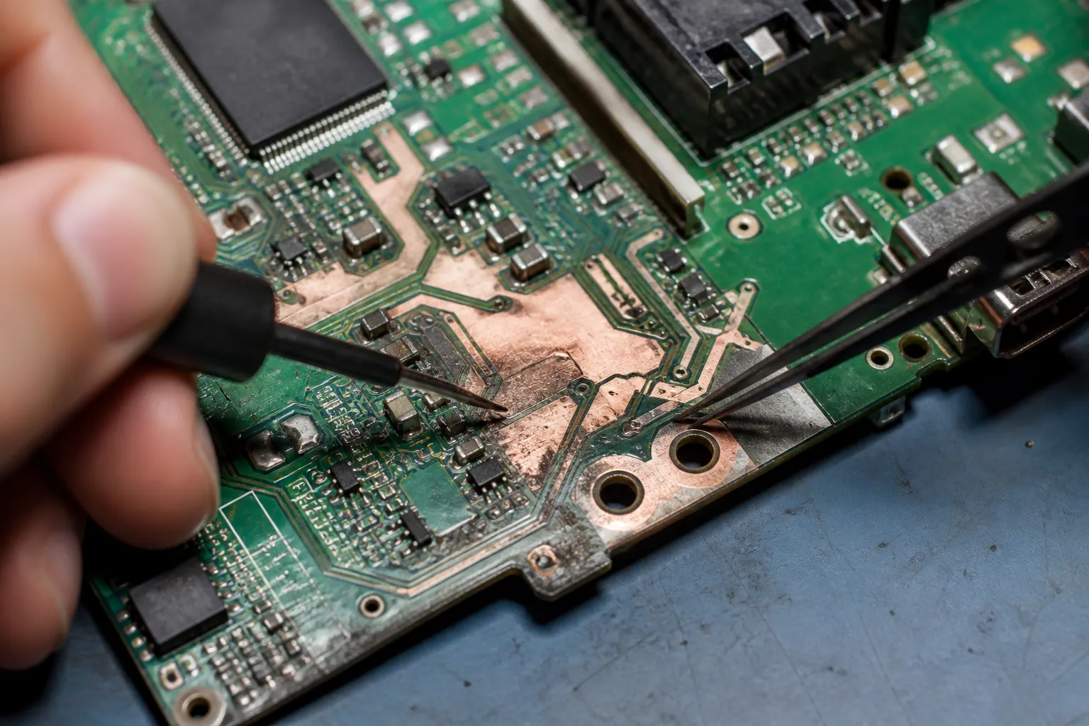
Inspection criteria also need to distinguish cosmetic oxidation from rejectable surface condition. A team that cannot tell the difference will either over-scrap usable boards or pass borderline copper because the discoloration looked minor under one lamp and severe under another. That is a process problem, not just a materials problem.
When adding solder mask is the cheaper engineering decision
Many no-mask ideas start as a simplification and end as hidden cost. The board may be slightly easier to route, easier to probe, or more convenient for a one-off modification. But if that choice increases assembly caution, handling requirements, inspection debate, or field sensitivity, the money returns later as yield loss and service time.
A mask opening should earn its place. If it does not create a real electrical, thermal, or mechanical benefit, covering the copper is usually the better DFM decision. The cost of adding mask is often lower than the cost of managing oxidation, paste spread, cosmetic fallout, and repeated operator judgment calls across a production run.
This is especially true for boards that are expected to sit in inventory, travel through multiple subcontractors, or face rework after assembly. The farther the board moves from a tightly controlled lab environment, the more valuable that mask barrier becomes.
A PCB without solder mask needs a reason, not just an exception
Leaving copper exposed on a PCB is not automatically wrong, but it should be treated as a deliberate engineering exception. If the open area supports a real function and the finish, spacing, storage, and inspection plan are defined, the design can be reliable. If the copper is exposed because the risk looked small on screen, oxidation is only the first warning sign. The more expensive problems usually show up later as inconsistent soldering, contamination-driven leakage, or rework that takes too much heat and too much time.
Can a PCB work without solder mask?
Yes, but only when the exposed copper is intentional and controlled. Test pads, contact zones, thermal interfaces, and some RF features may need open metal. A board with large unnecessary no-mask areas is much more vulnerable to oxidation, contamination, bridging, and handling damage.
Does exposed copper always become impossible to solder?
Not immediately. Fresh exposed copper may still solder well, especially on a quick prototype, but solderability gets less stable as the surface ages, absorbs contamination, or sees poor storage conditions. The risk is inconsistency, not just total failure.
Is oxidation the main reason to avoid a PCB without solder mask?
Oxidation is only part of the problem. Missing solder mask also removes spacing control around exposed metal, makes paste spread and accidental bridging more likely, and leaves the board more sensitive to residue, moisture, and rough handling during repair or inspection.
When is it acceptable to leave copper exposed on a PCB?
It is acceptable when the exposed area has a defined job, such as a contact surface, test pad, thermal interface, or controlled solderable region, and when the finish, spacing, storage, and inspection rules are chosen around that purpose.