What is IGBT?
IGBT stands for Insulated Gate Bipolar Transistor, which is a type of power semiconductor device that combines bipolar junction transistors (BJTs) and metal oxide semiconductor field-effect transistors (MOSFETs). IGBTs have high input impedance like MOSFETs and low voltage drop during conduction like giant transistors (GTRs). They are commonly used in applications where the DC voltage is 600V or higher, such as AC motors, inverters, power supplies, lighting circuits, and traction drives.
IGBTs are a core component of power electronics devices and are often referred to as the “CPU” of these devices. They are widely used in various fields such as rail transportation, smart grids, aerospace, electric vehicles, and new energy equipment.
Development Process of IGBT
Advancements in IGBT Technology in the 1980s
The concept of IGBT was first introduced in 1979 as a MOS-gated power switching device with a V-shaped trench gate. In the early 1980s, the DMOS (Double Diffused Metal Oxide Semiconductor) technology used for power MOSFET manufacturing was adopted for IGBTs, and the structure of the silicon chip was a thick NPT (Non-Punch-Through) design. Later, with the development of epitaxial technology on the silicon chip and the use of n+ buffer layers designed for a given blocking voltage, a significant improvement in parameter tradeoffs was achieved by adopting the PT (Punch-Through) structure.
Progress in IGBT Design in the 1990s
In the mid-1990s, the trench gate structure was reintroduced in a new concept of IGBT using a new etching process borrowed from large-scale integration (LSI) technology, but the chip structure was still PT. This new trench structure allowed for a compromise between on-state voltage and turn-off time. The chip structure of silicon also underwent a dramatic transformation from NPT to LPT (Light Punch-Through) structures, which improved the Safe Operating Area (SOA) similar to the evolution of the planar gate structure.
The transition from PT to NPT was the most fundamental and significant conceptual change. PT technology has a relatively high carrier injection coefficient, but it requires control of the minority carrier lifetime, which reduces transport efficiency. In contrast, NPT technology has good transport efficiency without killing minority carriers, but its carrier injection coefficient is relatively low. LPT technology, which is similar to soft punch-through or field-stop technology, replaced NPT technology and further improved the cost-performance tradeoff.
CSTBT and 5th Generation IGBT Modules
In 1996, the CSTBT (Carrier Stored Trench Gate Bipolar Transistor) enabled the realization of the 5th generation IGBT module. It used the LPT chip structure and a more advanced design with wide cell spacing. Currently, new concepts of IGBT devices with “reverse blocking type” or “reverse conducting type” functions are being studied to achieve further optimization.
IGBT power modules have evolved from composite power modules (PIM) to intelligent power modules (IPM), power electronic building blocks (PEBB), and power modules (IPEM) that use IC drivers, various driving protection circuits, high-performance IGBT chips, and new packaging technologies.
IGBT Structure
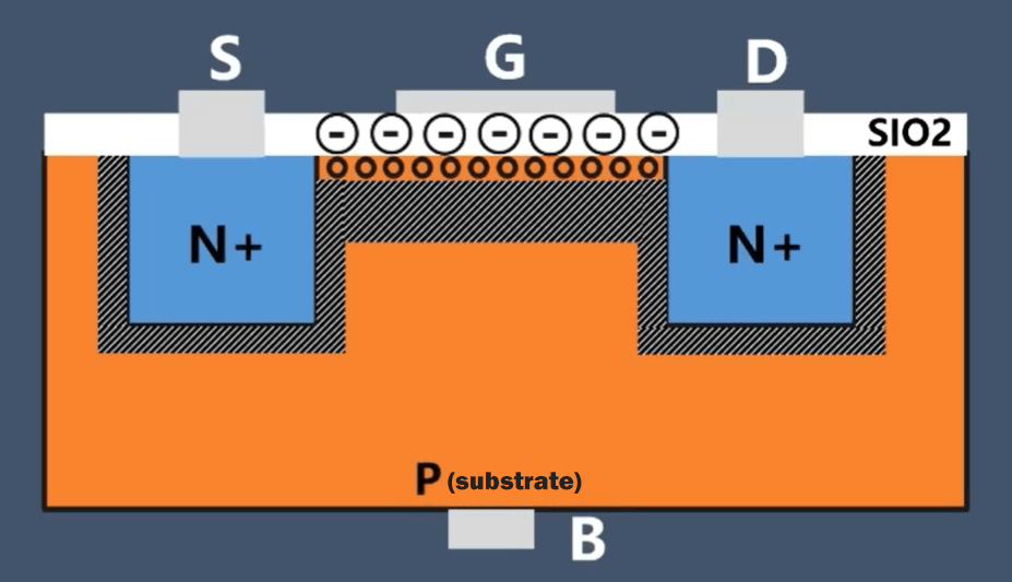
The left side of the IGBT diagram shows the structure of an N-channel enhancement insulated gate bipolar transistor. The N+ region is called the source region, and the electrode attached to it is called the source electrode (or emitter E). The N base is called the leakage region. The control area of the device is the gate region, and the electrode attached to it is called the gate electrode (or gate G). The channel is formed right next to the boundary of the gate region. The P-type region (including P+ and P- regions) between the C and E poles (where the channel is formed) is called the sub-channel region. The P+ region on the other side of the leakage region is called the drain injection region, which is a unique functional area of the IGBT. It forms a PNP bipolar transistor together with the leakage region and sub-channel region, acting as the emitter, injecting holes into the leakage region to modulate conductivity and reduce the on-state voltage of the device. The electrode attached to the drain injection region is called the drain electrode (or collector C).

The switching action of the IGBT is achieved by applying a forward gate voltage to form a channel, providing base current to the PNP (originally NPN) transistor, and turning on the IGBT. Conversely, applying a reverse gate voltage eliminates the channel, cuts off the base current, and turns off the IGBT. The driving method of the IGBT is basically the same as that of a MOSFET, only controlling the input gate N-channel MOSFET, so it has a high input impedance. When the channel of the MOSFET is formed, holes (minority carriers) are injected from the P+ base into the N- layer, modulating the conductivity of the N- layer and reducing its resistance, allowing the IGBT to have a low on-state voltage even at high voltages.
IGBT Working Principle
An IGBT works like a MOSFET, but in an IGBT, the drain of the MOSFET is replaced with the emitter of a BJT. This achieves the high input impedance of the MOSFET and the drive capability of the BJT. Now let’s see how IGBT works basing on the following 4 points:
Gate control of IGBT
IGBTs are turned on and off by applying a voltage to the gate. When a positive voltage is applied to the gate, holes are injected into the n-doped drift region, creating a conducting channel for current flow.
Current flow and threshold voltage
The amount of current that can flow through an IGBT is determined by the size of the conducting channel in the drift region, which is controlled by the gate voltage. When the gate voltage is decreased below a threshold level, the channel is cut off and no current can flow.
Parasitic thyristor structure and latch-up prevention
When the collector-emitter voltage is reverse-biased, a parasitic thyristor structure can form within the IGBT, leading to latch-up or device failure. To prevent this, IGBTs are designed with a lightly doped region near the collector to reduce the gain of the parasitic thyristor structure.
Tail current in IGBT
IGBTs also exhibit a tail current or a slow decay in the collector current after the gate voltage is turned off. This is due to the presence of minority carriers (holes) in the n-doped drift region that gradually recombine and reduce the current. The magnitude of the tail current is dependent on factors such as doping concentration, temperature, and device geometry.
IGBT Characteristics
Static Characteristics
The static characteristics of an IGBT mainly include the volt-ampere characteristics and transfer characteristics.
Volt-Ampere
The volt-ampere characteristics of an IGBT refer to the relationship between the collector-emitter current and the gate-source voltage when the gate-source voltage Ugs is used as the reference variable. The output collector-emitter current is controlled by the gate-source voltage Ugs, with higher Ugs resulting in larger Id. It is similar to the output characteristics of a GTR and can be divided into the saturation region (1), the amplification region (2), and the breakdown characteristics (3). In the off-state of an IGBT, the forward voltage is borne by the J2 junction, while the reverse voltage is borne by the J1 junction. If there is no N+ buffer region, the forward and reverse blocking voltages can be at the same level. However, after the N+ buffer region is added, the reverse blocking voltage can only reach tens of volts, which limits the application range of the IGBT.
Transfer
The transfer characteristics of an IGBT refer to the relationship between the output collector-emitter current Id and the gate-source voltage Ugs. It is the same as the transfer characteristics of a MOSFET. When the gate-source voltage is less than the threshold voltage Ugs(th), the IGBT is in the off-state. Within most of the range of collector-emitter current when the IGBT is conducting, Id is linearly related to Ugs. The maximum gate-source voltage is limited by the maximum collector-emitter current, and its optimal value is generally around 15V.
Dynamic Characteristics
The dynamic characteristics of an IGBT are also called switching characteristics, which can be divided into two parts: switching speed and switching losses.
The switching characteristics of an IGBT refer to the relationship between the collector-emitter current and the collector-source voltage. When an IGBT is in the conducting state, its PNP transistor has a low value of B due to its wide base. Although the equivalent circuit is a Darlington structure, the current flowing through the MOSFET becomes the main part of the total current of the IGBT. At this time, the on-state voltage Uds(on) can be expressed as follows:
Uds(on) = Uj1 + Udr + IdRoh
where Uj1 is the forward voltage of the J1 junction with a value of 0.7-1V, Udr is the voltage drop on the extension resistance Rdr, and Roh is the channel resistance. The on-state current Ids can be expressed as follows:
Ids=(1+Bpnp)Imos
where Imos is the current flowing through the MOSFET. Because of the conductivity modulation effect in the N+ region, the on-state voltage drop of the IGBT is small, and the on-state voltage drop of a 1000V IGBT is 2-3V. When the IGBT is in the off-state, only a small leakage current exists.
During the turn-on process of an IGBT, most of the time it operates as a MOSFET. It is only in the later stage of the decrease of the collector-source voltage Uds that the PNP transistor switches from the amplification region to saturation, which increases the delay time. td(on) is the turn-on delay time, and tri is the current rise time. In practical applications, the turn-on time of the collector-emitter current, ton, is the sum of td(on) and tri, and the fall time of the collector-source voltage is composed of tfe1 and tfe2.
Types of IGBT
Low-power IGBT
IGBT is generally used in the range of 600V, 1KA, and 1KHz or above. To meet the development needs of the home appliance industry, companies such as Motorola, ST Semiconductor, and Mitsubishi have introduced low-power IGBT products that are practical for home appliances such as microwave ovens, washing machines, induction cookers, electronic rectifiers, and cameras.
U-IGBT
U (trench structure) – IGBT is a structure that has a trench-shaped gate formed inside the chip cell by carving grooves on the chip core. After adopting the trench structure, the cell size can be further reduced, the channel resistance can be reduced, the current density can be improved, and the smallest product with the same rated current and chip size can be manufactured. There are many companies that produce various U-IGBT products, which are suitable for low-voltage driving and surface mount requirements.
NPT-IGBT
NPT (non-punch-through) – IGBT uses thin silicon wafer technology to replace the thick high-resistance epitaxial layer with ion implantation into the emitter region, which can reduce production costs by about 25%. The higher the withstand voltage, the greater the cost difference. It has superior characteristics in performance, high speed, low loss, positive temperature coefficient, no latch-up effect, and the highest reliability in designing IGBT from 600-1200V. Siemens can provide 600V, 1200V, 1700V series products and 6500V high-voltage IGBT. It has also launched low-saturation voltage drop DLC-type NPT-IGBT. Infineon, Harris, Intersil, Toshiba, and other companies have also developed NPT-IGBT and module series. Fuji Electric, Motorola, and others are currently developing it, and the NPT type is becoming the direction of IGBT development.
SDB-IGBT
Given that manufacturers currently attach great importance to the development of IGBT, Samsung, QuickLogic, and other companies use SDB (silicon wafer direct bonding) technology to produce the fourth generation of high-speed IGBT and module series products on the IC production line. The characteristics are high speed, low saturation voltage drop, low tail current, and positive temperature coefficient, which are excellent in the 600V and 1200V voltage range, divided into two systems: UF and RUF.
Ultra-fast IGBT
The research and development focus of international rectifier IR company is to reduce the tail effect of IGBT and make it quickly turn off. The developed ultra-fast IGBT can minimize the tail effect, with a turn-off time of no more than 2000ns. By using a special high-energy irradiation layering technology, the turn-off time can be below 100ns, and the tail is even shorter. The key products are designed for motor control, with six models available, and can also be used in high-power power converter.
IGBT/FRD
IR company has introduced two new devices that combine FRD (fast recovery diode) with IGBT. The effective combination of IGBT/FRD reduces the switching losses by 20%. It adopts TO-247 package and has a rated specification of 1200V, 25, 50, 75, and 100A. It is used for motor drive and power conversion. The new technology based on IGBT and FRD is conducive to the parallel connection of devices, achieving more uniform temperature in multi-chip modules and improving overall reliability.
IGBT Modules
An IGBT module is a type of modular semiconductor product that consists of IGBT chips and freewheeling diode (FWD) chips packaged together using specific circuit interconnections. These modules are directly used in various devices such as variable frequency drives (VFDs) and inverter modules. They are known for their energy-saving features, ease of installation and maintenance, and stable heat dissipation. Most of the IGBTs available in the market are in the form of these modular products.
From PIM to IPEM: The Evolution of IGBT Modules
IGBT modules use IC drivers and various driver protection circuits, high-performance IGBT chips, and new packaging technologies. They have evolved from the Power Integrated Module (PIM) to the Intelligent Power Module (IPM), Power Electronic Building Blocks (PEBB), and Integrated Power Electronic Modules (IPEM). PIMs have evolved towards high voltage and high current applications with a product range of 1200-1800A/1800-3300V. IPMs are mainly used for variable frequency drives, while 600A/2000V IPMs have been used in electric locomotive VVVF inverters. PEBBs use a planar low-inductance packaging technology with high-current IGBT modules as active devices, which are used in ship missile launchers. IPEMs use co-fired ceramic chip multi-chip module technology to assemble PEBBs, which greatly reduces circuit wiring inductance and improves system efficiency. The second generation of IPEMs has been successfully developed, where all passive components are embedded in the substrate in the form of buried layers.
Intelligent and modular design is becoming a development hotspot for IGBTs. With the promotion of energy conservation and environmental protection concepts, these products will become more prevalent in the market.
IGBT vs MOSFET
| Feature | IGBT | MOSFET |
|---|---|---|
| Full name | Insulated Gate Bipolar Transistor | Metal-Oxide-Semiconductor Field-Effect Transistor |
| Number of leads | 3 | 3 |
| Lead names | Collector (C), Emitter (E), Gate (G) | Source (S), Drain (D), Gate (G) |
| Breakdown Voltage | Up to 1200V | Lower than IGBTs |
| Collector Saturation Current | Over 1500A | Lower than IGBTs |
| Switching Speed | between 1 kHz and 20 kHz | 20 to 200 picoseconds |
| Conduction Losses | Lower | Higher |
| Switching Losses | Higher | lower |
| Thermal Stability | Better | Worse |
| Safe Operating Area (SOA) | Larger | Smaller |
| Advantages | High breakdown voltage, high collector saturation current, good high-frequency performance | Good thermal stability, large safe operating area |
| Disadvantages | Slow switching speed, high switching losses | Low breakdown voltage, low operating current |
| Typical applications | Inverters, motor drives, power supplies for high voltage and high current applications | Switching power supplies, DC-DC converters, power amplifiers |
How to Check IGBT with Multimeter?
To check an IGBT with a multimeter, you need to follow the steps below:
Determine the polarity:
Set the multimeter to R×1KΩ and measure the resistance between each of the three pins. The pin with infinite resistance to the other two pins after swapping the multimeter leads is the gate (G) pin. Then, measure the resistance again with the other two pins, and the pin with a lower resistance is the collector (C), while the other one is the emitter (E).
Test for functionality:
Set the multimeter to R×10KΩ and connect the black probe to the collector (C) and the red probe to the emitter (E) of the IGBT. The multimeter pointer should be at zero. Touch both the gate (G) and the collector (C) pins simultaneously with your fingers, and the IGBT should turn on, and the multimeter pointer should move towards a lower resistance value and stay there. Then, touch both the gate (G) and emitter (E) pins with your fingers, and the IGBT should turn off, and the multimeter pointer should return to zero. If this happens, then the IGBT is working correctly.
Precautions:
Use any pointer-type multimeter to test IGBTs. Always set the multimeter to R×10KΩ when testing for functionality, as the lower resistance settings do not have enough voltage to trigger the IGBT. This method can also be used to check the power MOSFETs (P-MOSFET) for functionality.
IGBT Application
As one of the important high-power mainstream devices of power electronics, IGBT has been widely used in household appliances, transportation, power engineering, renewable energy and smart grid and other fields.
In industrial applications, such as traffic control, power conversion, industrial motors, uninterruptible power supplies, wind power and solar energy equipment, and frequency converters for automatic control.
In consumer electronics, IGBTs are used in home appliances, cameras and mobile phones.