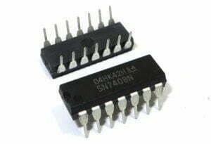
What is LM339 Comparator?
LM339 is a common integrated circuit that contains four independent voltage comparators inside, making it a quad differential comparator. It is mainly used in high-voltage digital logic gate circuits. LM339 can be easily used to form various voltage comparator circuits and oscillator circuits.
LM339 Pinout
The following figure is the LM339 pin diagram:

Pinout Description
| Pin Number | Symbol | Function |
|---|---|---|
| 1 | OUTPUT2 | Output 2 |
| 2 | OUTPUT1 | Output 1 |
| 3 | V+ | Positive Supply |
| 4 | INPUT1- | Inverting Input 1 |
| 5 | INPUT1+ | Non-inverting Input 1 |
| 6 | INPUT2- | Inverting Input 2 |
| 7 | INPUT2+ | Non-inverting Input 2 |
| 8 | INPUT3- | Inverting Input 3 |
| 9 | INPUT3+ | Non-inverting Input 3 |
| 10 | INPUT4- | Inverting Input 4 |
| 11 | INPUT4+ | Non-inverting Input 4 |
| 12 | GND | Ground |
| 13 | OUTPUT4 | Output 4 |
| 14 | OUTPUT3 | Output 3 |
LM339 Parameters
| Attributes | Value |
|---|---|
| Manufacturer | STMicroelectronics |
| VIO | ±2 mV |
| IOS | 150 nA |
| ICC | 1.3 mA |
| IB | 250 nA |
| Common-Mode Range | 0V to Vcc-1.5V |
| Vcc | 2V to 36V (single-supply); ±1V to ±18V (dual-supply) |
| Vos | 5 mV |
| Number of Channels | 4 |
| Min. Temp | 0 ℃ |
| Max. Temp | +70℃ |
| Package | TSSOP-14, PDIP-14, SOIC-14 |
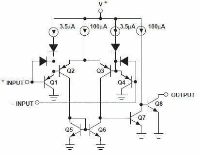
LM339 Circuit Diagram
How LM339 Comparator Works?
The operating principle of LM339 is similar to that of other comparator ICs, with each comparator having three pins, namely: inverting (-IN), non-inverting (+IN), and output.
To understand the working principle of LM339, let’s use one of its comparators as an example.
We take two input voltages, namely V1 and V2. Now, these voltages are compared using the comparator and the output is provided as Vo. Voltage V1 is connected to the non-inverting (+IN) input (pin 5) of the comparator, while voltage V2 is connected to the inverting (-IN) input (pin 4).
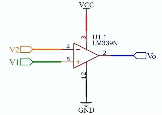
If the voltage at the inverting (-IN) input (V2) is greater than that at the non-inverting (+IN) input (V1), then the output will be logic low.
V2>V1, Vo = 0V or GND
If the voltage at the non-inverting (+IN) input (V1) is greater than that at the inverting (-IN) input (V2), then the output will be logic high.
V1>V2, Vo = VCC
LM339 Equivalent Models
LM311, LM324, LM397, LM139, LM239, LM2901, etc.
LM339 Application
- Oscillator, Crystal controlled oscillator
- Single-limit comparators, hysteresis comparators, dual-limit comparators
- Voltage comparator, Negative Reference Comparator
- Measuring instrument
- High-voltage digital logic gate circuits
- Rlectricity regulation
- Logic Voltage Conversion
- Measuring instrument
- Driver CMOS, Driver TTL
- Low Frequency Operational Amplifier
- Sensor amplifier
- Zero crossing detector
Engineering checks for LM339 comparator pinout and open-collector output design
Before using LM339 comparator pinout and open-collector output design in a PCB, firmware, repair, or validation workflow, confirm the details that usually decide whether the design works reliably instead of only reading the headline specification.
LM339 Input, Output, and Pull-Up Checks
| Area | What to check | Why it matters |
|---|---|---|
| Input range | Check common-mode voltage, offset, hysteresis, and reference divider tolerance | Comparator errors often come from input range assumptions |
| Output stage | Add a pull-up resistor sized for speed, current, and logic voltage | LM339 outputs are open-collector and cannot drive high without a pull-up |
| Noise control | Use hysteresis, filtering, grounding, and decoupling near the device | Slow or noisy inputs can make comparator outputs chatter |