Choosing the Right EDA Software for Your IC Board Design Project

Table of Contents

A person working on an IC circuit board with EDA software displayed on a monitor.

In the dynamic and complex realm of Integrated Circuit (IC) board design projects, the choice of Electronic Design Automation (EDA) software stands as a linchpin for success. EDA software has revolutionized the IC design landscape, enabling engineers to transform abstract ideas into tangible, high – performance circuits.​

However, with a plethora of EDA software options available in the market, each boasting a unique set of features, capabilities, and price points, the selection process can be daunting. This article aims to demystify the process of choosing the right EDA software for your IC board design project, providing you with a comprehensive guide to make an informed decision.

What is EDA Software?

Definition and Basics

EDA software, short for Electronic Design Automation software, is a suite of tools that have become indispensable in the design and development of electronic systems, particularly in the creation of integrated circuits (ICs). In essence, it is a virtual workspace where engineers can transform their ideas for electronic components into a fully – fledged, functional design.​

Before the advent of EDA software, the design of electronic circuits was a painstakingly manual process. Engineers had to draw circuit diagrams by hand, calculate component values manually, and physically build and test prototypes at every stage. This was not only time – consuming but also highly error – prone. EDA software revolutionized this process by automating many of these tasks. It provides a platform where engineers can use digital representations of components and circuits, and the software takes care of the complex calculations, simulations, and optimizations.​

For example, in the design of a simple microcontroller – based circuit, an engineer can use EDA software to select and place virtual components such as the microcontroller, resistors, capacitors, and other peripherals on a virtual canvas. The software then automatically calculates the electrical parameters and connections between these components, eliminating the need for manual calculations.

A diagram illustrating the process of Electronic Design Automation (EDA), showing the stages of logical design, circuit simulation, physical layout, and verification.
A visual breakdown of the key functions within EDA software, from initial logical design to final verification

Benefits

The importance of selecting the right EDA tools cannot be overstated. Firstly, it directly impacts the efficiency of the design process. A well – suited EDA software can streamline tasks such as schematic capture, layout design, and simulation, reducing the time spent on mundane and error – prone manual operations. For example, advanced EDA tools with automated routing algorithms can significantly cut down the time required to route interconnects in a complex IC layout, which might otherwise take days or even weeks if done manually.
 
Secondly, the quality of the final IC design is closely tied to the capabilities of the EDA software. High – end EDA tools offer sophisticated simulation and verification features. These allow engineers to accurately predict how the designed IC will perform under various real – world conditions, such as different temperature ranges, power supplies, and signal frequencies. By catching design flaws early in the development cycle through comprehensive simulations, costly re – design iterations and potential product failures can be avoided.
 
Moreover, in an industry where technological advancements are rapid and market competition is fierce, choosing the right EDA software can give a project a competitive edge. It enables the implementation of the latest design techniques and standards, ensuring that the resulting ICs are not only functional but also state – of – the – art in terms of performance, power consumption, and size.

Core Functions

  1. Logical Design
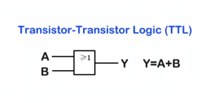
    • At the heart of any IC design is the logical design phase. EDA software allows engineers to define the functionality of the circuit using hardware description languages (HDLs) like Verilog or VHDL. Through these languages, engineers can describe the behavior of the digital components in the circuit, such as how flip – flops store data, how logic gates perform operations like AND, OR, and NOT, and how different components interact with each other. For instance, when designing a digital clock circuit, the engineer can use HDL code in the EDA software to define the counter logic that keeps track of seconds, minutes, and hours, and the display logic that shows the time on an output device.
  1. Circuit Simulation
    • Circuit simulation is another crucial function of EDA software. It enables engineers to test the behavior of the designed circuit before it is physically fabricated. By running simulations, engineers can analyze how the circuit responds to different input signals, power supplies, and operating conditions. For example, in the design of a power amplifier circuit, simulation in EDA software can show how the amplifier behaves under different input signal amplitudes, frequencies, and load conditions. This helps in identifying issues like signal distortion, power consumption problems, and thermal issues early in the design process, saving both time and cost.
  1. Layout and Routing
    • Once the logical design and simulation are complete, the next step is to create the physical layout of the IC. EDA software provides layout tools that help engineers place the various components of the circuit on the chip’s surface and route the interconnecting wires between them. In a high – density IC with millions of transistors, the layout and routing process is extremely complex. EDA software uses algorithms to optimize the placement of components to minimize the chip area and the length of interconnecting wires, which in turn reduces signal delay and power consumption. For example, in a modern smartphone’s application processor chip, the EDA software’s layout and routing tools ensure that billions of transistors and their connections are arranged in a way that maximizes performance while keeping the chip size compact.
  1. Verification and Validation
    • Verification and validation are essential to ensure that the designed IC meets all the required specifications. EDA software offers a range of verification tools, including formal verification, which uses mathematical methods to prove that the design meets its specified requirements, and simulation – based verification, which checks the design’s functionality through various test cases. Validation tools, on the other hand, ensure that the fabricated IC behaves as expected in real – world applications. For example, in the design of a safety – critical automotive IC, rigorous verification and validation using EDA software are crucial to ensure that the IC functions correctly in all possible driving conditions and does not pose any safety risks.

Key Factors to Consider When Selecting EDA Software

Design Requirements

Functionality Needed

The functionality of EDA software is a fundamental consideration. Different IC board design projects have diverse requirements. For example, if you are designing a high – speed digital IC for a data – center networking application, you will need EDA software with advanced high – speed signal integrity analysis capabilities. This includes features such as impedance matching analysis, crosstalk simulation, and signal delay calculation. Tools like Cadence Allegro offer comprehensive high – speed design capabilities, allowing engineers to accurately model and analyze the behavior of high – speed signals in complex digital circuits.
 
On the other hand, for analog IC design, such as a power management IC, the EDA software should have strong analog simulation features. It should be able to accurately model components like transistors, capacitors, and inductors in the analog domain, and perform simulations for parameters like power consumption, voltage regulation, and noise characteristics. Tools like Mentor Graphics’ Analog FastSPICE are well – known for their high – accuracy analog simulation capabilities, making them suitable for analog – intensive IC design projects.

Complexity of the Project

The complexity of the IC board design project is another crucial factor. Simple projects with a few dozen components and basic functionality can be handled by less – feature – rich EDA software. For instance, if you are designing a basic microcontroller – based development board with a few peripheral components like LEDs, buttons, and a serial communication interface, entry – level EDA tools such as KiCad can be sufficient. KiCad offers basic schematic capture, layout design, and some simple simulation capabilities, making it an affordable and easy – to – use option for small – scale projects.
 
However, for large – scale, complex projects, such as the design of a multi – core system – on – a – chip (SoC) with millions of transistors and multiple functional blocks like CPUs, GPUs, and memory controllers, high – end EDA software is essential. These tools need to handle the complexity of hierarchical design, massive data management, and advanced verification techniques. Tools like Synopsys’ Design Compiler and IC Compiler are designed to handle such large – scale, complex IC designs. They offer features like hierarchical synthesis, physical design optimization, and formal verification, which are crucial for ensuring the success of complex SoC designs.

Ease of Use

Learning Curve

The learning curve associated with EDA software can significantly impact the project timeline, especially if the engineering team is new to the tool. For beginners or teams with limited EDA experience, a software with a gentle learning curve is highly desirable. Some EDA tools are designed with user – friendliness in mind, offering intuitive interfaces, comprehensive tutorials, and helpful wizards. For example, EasyEDA is an online – based EDA tool that is particularly popular among hobbyists and students. It has a simple and intuitive interface, and provides step – by – step tutorials for basic IC design tasks such as schematic capture and PCB layout. This allows new users to quickly get up to speed and start their design projects without spending a long time on learning the software.
 
In contrast, some high – end EDA tools, although powerful, can have a steep learning curve. These tools often come with a vast array of advanced features and complex workflows. For example, some enterprise – level EDA software used in large – scale semiconductor companies may require engineers to undergo extensive training to master all its capabilities. While the investment in learning these tools can pay off in terms of the advanced design and verification capabilities they offer, it’s important to consider the time and resources required for training, especially in projects with tight schedules.

User Interface

A well – designed user interface (UI) can greatly enhance the user experience and design efficiency. An intuitive UI makes it easier for engineers to navigate through the various functions of the EDA software. For example, a software with a clear and organized menu structure, where different design tasks such as schematic capture, layout, and simulation are easily accessible, can save a lot of time. Altium Designer is known for its user – friendly interface. It has a unified design environment where users can seamlessly switch between schematic design and PCB layout. The interface also provides real – time feedback, such as highlighting potential design errors as the user is working, which helps in catching mistakes early and improving the overall design quality.
 
Moreover, a customizable UI can be a great advantage for experienced users. They can arrange the workspace, toolbars, and panels according to their preferences and work habits. This allows them to streamline their workflow and work more efficiently. Some EDA software, like Xilinx ISE (Integrated Software Environment) for FPGA design, offers a certain degree of UI customization. Engineers can customize the layout of the project navigator, source code editor, and simulation windows to suit their specific design tasks and preferences.

Complexity of the Project

The complexity of the IC board design project is another crucial factor. Simple projects with a few dozen components and basic functionality can be handled by less – feature – rich EDA software. For instance, if you are designing a basic microcontroller – based development board with a few peripheral components like LEDs, buttons, and a serial communication interface, entry – level EDA tools such as KiCad can be sufficient. KiCad offers basic schematic capture, layout design, and some simple simulation capabilities, making it an affordable and easy – to – use option for small – scale projects.
 
However, for large – scale, complex projects, such as the design of a multi – core system – on – a – chip (SoC) with millions of transistors and multiple functional blocks like CPUs, GPUs, and memory controllers, high – end EDA software is essential. These tools need to handle the complexity of hierarchical design, massive data management, and advanced verification techniques. Tools like Synopsys’ Design Compiler and IC Compiler are designed to handle such large – scale, complex IC designs. They offer features like hierarchical synthesis, physical design optimization, and formal verification, which are crucial for ensuring the success of complex SoC designs.

Compatibility

With Other Tools

In modern IC design workflows, EDA software often needs to work in tandem with other design tools. Compatibility with other tools, such as Computer – Aided Design (CAD) and Computer – Aided Manufacturing (CAM) tools, is crucial for seamless data transfer and efficient design processes. For example, in the design of an IC board, the EDA software may need to export the layout data to a CAM tool for manufacturing. If the EDA software is not compatible with the CAM tool, it can lead to data conversion issues, errors in manufacturing, and delays in the project. EAGLE, an EDA tool, has good compatibility with various CAM software. It can export Gerber files, which are the standard format for PCB manufacturing, in a way that is easily readable by most CAM systems, ensuring a smooth transition from the design phase to the manufacturing phase.
 
In addition, compatibility with other EDA tools within the same design ecosystem can also be beneficial. For instance, in a large – scale IC design project, different teams may be using different EDA tools for different aspects of the design, such as one team using Synopsys tools for front – end design and another using Cadence tools for back – end design. In such cases, the ability of these tools to exchange data and work together is essential. Many EDA vendors are now working on improving interoperability between their tools, often through industry – standard data formats and interfaces, to enable seamless collaboration across different design phases and teams.

With Hardware

The compatibility of EDA software with hardware is another important consideration. This includes compatibility with the target hardware on which the designed IC will be implemented, as well as the hardware used for running the EDA software itself. For example, if you are designing an IC for a specific FPGA (Field – Programmable Gate Array) device, the EDA software must be compatible with that FPGA family. Xilinx Vivado is specifically designed to be compatible with Xilinx FPGA devices. It provides device – specific libraries, synthesis and implementation tools that are optimized for Xilinx FPGAs, ensuring that the designed IC can be successfully programmed onto the target device.
 
On the other hand, the EDA software also needs to be compatible with the computer hardware on which it runs. High – end EDA tools, especially those used for complex simulations and large – scale designs, often require significant computational resources. They need to be compatible with high – performance workstations or servers with multi – core processors, large amounts of RAM, and powerful graphics cards. For example, some advanced EDA simulation tools may not run smoothly on a standard desktop computer with limited resources, but will perform optimally on a workstation with a high – end CPU, 64GB or more of RAM, and a professional – grade graphics card.

Cost

Licensing Model

EDA software comes with various licensing models, each with its own cost implications. One common model is the per – user license. In this model, the software vendor charges a fee for each user who will be using the EDA software. This can be suitable for small teams where the number of users is well – defined. For example, a small startup with a team of 5 – 10 engineers may find a per – user license for an EDA tool like Altium Designer to be a cost – effective option. The cost per user may vary depending on the features and version of the software, but it allows the company to control the software costs based on the number of actual users.
 
Another model is the per – project license. With this model, the license fee is based on each individual design project. This can be beneficial for companies that work on a limited number of projects at a time. For instance, a design – services company that takes on a few high – value IC design projects may prefer a per – project license. The software vendor may charge a flat fee for each project, regardless of the number of engineers working on it, which can be more cost – effective for projects with large teams.
 
Subscription – based licensing has also become increasingly popular in recent years. In this model, the user pays a recurring fee, usually on a monthly or annual basis, to use the EDA software. This model offers several advantages, such as access to the latest software updates and features without having to pay for a major upgrade. For example, some EDA vendors offer subscription – based licenses for their tools, which can be more affordable for small and medium – sized enterprises (SMEs) that may not have the budget for a large upfront software purchase. It also allows companies to scale their software usage up or down based on their project needs, as they can easily cancel or renew the subscription.

Total Cost of Ownership

When evaluating the cost of EDA software, it’s important to consider the total cost of ownership (TCO), which includes not only the initial purchase or licensing fee but also other associated costs. The maintenance cost is one such factor. EDA software vendors often charge a maintenance fee, usually a percentage of the initial software cost, to provide technical support, bug fixes, and software updates. For example, a high – end EDA tool may have a maintenance fee of 15 – 20% of the license cost per year. This ensures that the software remains up – to – date and compatible with the latest industry standards and hardware.
 
Upgrade costs also need to be factored in. As technology evolves, EDA software vendors release new versions with enhanced features and capabilities. Upgrading to a new version may require an additional fee. For example, a major upgrade of an EDA tool may cost a significant portion of the original license price. It’s important to consider these upgrade costs over the long term, especially if the software is expected to be used for several years.
 
In addition, there may be costs associated with training the engineering team to use the EDA software effectively. This can include the cost of in – house training sessions, online courses, or sending employees to vendor – sponsored training programs. For example, if a company purchases a new, complex EDA tool, it may need to invest in training courses for its engineers, which can add to the overall cost of using the software. All these factors – licensing fees, maintenance costs, upgrade costs, and training costs – should be considered when calculating the total cost of ownership of an EDA software, to make an informed decision that aligns with the project’s budget and long – term requirements.

Popular EDA Software in the Market

Cadence

Cadence stands as a titan in the EDA software landscape, offering a comprehensive suite of tools that cater to a wide range of IC design requirements. One of its major strengths lies in its prowess in both analog and digital circuit design and verification.
 
In the realm of analog and mixed – signal IC design, Cadence’s tools are highly regarded. For instance, its Virtuoso ADE Product Suite provides a comprehensive environment for analog circuit design. Engineers can create custom device models, perform in – depth simulations, and precisely tune parameters. This is crucial for applications such as designing high – performance amplifiers for audio equipment or precision analog – to – digital converters (ADCs) in data – acquisition systems. The suite’s advanced simulation capabilities can accurately model the behavior of analog components under various operating conditions, ensuring that the final design meets the stringent requirements of real – world applications.
A splash screen for Cadence Virtuoso EDA software
The splash screen for Cadence's Virtuoso Front to Back Design Environment
When it comes to digital IC design, Cadence offers tools like the Genus Synthesis Solution. This tool is focused on logic synthesis and plays a vital role in optimizing the power, performance, and area (PPA) of digital circuits. It uses sophisticated algorithms to transform high – level descriptions of digital circuits into optimized gate – level netlists. For example, in the design of a high – speed microprocessor, Genus can optimize the circuit to achieve maximum processing speed while minimizing power consumption and chip area, which are critical factors in modern digital IC design.
 
Cadence’s Spectre Circuit Simulator is another flagship product. It is renowned for its SPICE – level accuracy in circuit simulation, making it an essential tool for RF (Radio Frequency) and other high – performance applications. Whether it’s designing a 5G communication chip or a high – frequency radar transceiver, Spectre can accurately simulate the behavior of RF circuits, taking into account factors such as signal attenuation, impedance matching, and electromagnetic interference.

Synopsys

Synopsys has firmly established itself as a leader in the digital design domain, with a suite of tools that are industry – standards in many aspects of the IC design process.
 
In the area of logic synthesis, Synopsys’ Design Compiler is a dominant force. It has been the go – to tool for engineers for decades, being supported by over 60 semiconductor vendors and more than 380 process libraries. Design Compiler enables IC designers to translate Register – Transfer – Level (RTL) descriptions into optimized gate – level circuits. It takes into account various design constraints such as timing, power, and area, and uses a wide range of optimization techniques like logic restructuring, resource sharing, and gate – sizing to achieve the best possible design. For example, when designing a complex system – on – a – chip (SoC) with multiple functional blocks, Design Compiler can efficiently synthesize the digital logic of each block, ensuring that the overall SoC meets its performance targets.
IC Compiler II Anchor in Synopsys Design Platform
IC Compiler II Anchor in Synopsys Design Platform | Photo by Synopsys
The company’s verification tools are also highly regarded. VCS (Verilog Compiled Simulator) is a high – performance simulation engine that supports multiple hardware description languages, including Verilog, SystemVerilog, and VHDL. It can handle large – scale designs with ease, making it suitable for the verification of complex ICs such as advanced microprocessors and high – end FPGAs. VCS offers features like fast simulation speed, high – accuracy waveform generation, and advanced debugging capabilities, which are essential for ensuring the functionality of the designed IC.
 
In the physical design realm, Synopsys’ IC Compiler II is a state – of – the – art tool. It is responsible for the layout and routing of digital circuits on the chip. IC Compiler II uses advanced algorithms to optimize the placement of components and the routing of interconnecting wires. It can handle the complex challenges of modern IC design, such as dealing with high – density layouts, multi – voltage domains, and complex power – distribution networks. For example, in the design of a high – performance graphics processing unit (GPU), IC Compiler II can ensure that the billions of transistors and their connections are arranged in a way that maximizes performance and minimizes signal delay.

Mentor Graphics (Siemens)

Since its acquisition by Siemens, Mentor Graphics has continued to evolve and expand its footprint in the EDA market, with its tools finding wide – spread application in both PCB and IC design.
 
In the PCB design space, Mentor Graphics’ PADS software is well – known. It offers a comprehensive set of features for PCB layout and design. PADS allows engineers to create detailed PCB layouts, manage component placement, and route traces with ease. It also provides advanced features for signal integrity analysis, which is crucial for high – speed PCB designs. For example, in the design of a high – speed motherboard for a server, PADS can analyze and optimize the signal paths to ensure that data can be transmitted at high speeds without significant signal degradation.
A splash screen for Mentor Graphics PADS Schematic Design software
The splash screen for Mentor Graphics PADS Schematic Design
In the IC design domain, Mentor Graphics offers tools like Calibre. Calibre is a powerful physical verification tool that plays a crucial role in ensuring the manufacturability of IC designs. It can perform design rule checking (DRC), layout vs. schematic (LVS) verification, and parasitic extraction. These functions are essential for detecting and correcting any design flaws that could lead to manufacturing failures. For example, Calibre can check if the IC layout adheres to the strict manufacturing rules of a particular semiconductor foundry, and if there are any short – circuits or open – circuits in the layout.
 
Mentor Graphics also offers tools for analog and mixed – signal IC design, such as Eldo. Eldo is a circuit simulator that provides accurate simulation of analog and mixed – signal circuits. It can handle complex analog designs, including those with multiple voltage domains and high – frequency components, making it suitable for applications such as power management ICs and high – speed communication interfaces.

Other Notable Software

  1. KiCad
KiCad is an open – source EDA software that has gained popularity, especially among hobbyists, students, and small – scale design teams. It offers a basic yet comprehensive set of tools for IC board design. KiCad allows users to create schematics, design PCB layouts, and perform some simple simulations. One of its main attractions is its user – friendly interface and low – cost nature (since it’s open – source). For example, a hobbyist interested in designing a simple microcontroller – based project, like a home – made weather station, can use KiCad to quickly design the circuit schematic and layout the PCB, all without having to invest in expensive commercial EDA software.
  1. Altium Designer
Altium Designer is known for its ease of use and its ability to handle a wide range of design projects, from simple to moderately complex. It provides a unified design environment where users can seamlessly move between schematic capture, PCB layout, and 3D modeling. This software is popular among small to medium – sized enterprises (SMEs) and design – focused startups. For instance, a startup developing a new consumer electronics product, such as a portable audio player, can use Altium Designer to design the entire circuit board, visualize how the components will be arranged in 3D, and ensure that the design is manufacturable.
  1. Xilinx ISE (Integrated Software Environment) and Vivado
These are EDA tools specifically tailored for Xilinx FPGA (Field – Programmable Gate Array) design. Xilinx ISE has been a long – standing tool in the FPGA design community, offering a suite of features for FPGA synthesis, implementation, and debugging. Vivado, on the other hand, is Xilinx’s next – generation design suite. It offers enhanced features such as high – level synthesis (HLS), which allows engineers to describe FPGA designs in a more abstract way, using languages like C, C++, and SystemC. These tools are essential for engineers working on projects that involve Xilinx FPGAs, such as developing custom – designed hardware accelerators for data – center applications or implementing real – time control systems using FPGAs.

Making the Decision

Case Studies​

  • Case 1: High – Speed Digital IC Design for a Networking Application
A company was tasked with designing a high – speed digital IC for a next – generation data – center networking switch. The project required handling data rates of up to 100 Gbps. The design team initially considered several EDA software options. They evaluated the functionality of each software, focusing on its high – speed signal integrity analysis capabilities.
Cadence Allegro was chosen due to its advanced features in this area. It could accurately simulate the behavior of high – speed signals, taking into account factors such as signal attenuation, crosstalk, and impedance matching. During the design process, Allegro’s simulation tools helped the team identify and rectify potential signal integrity issues early on. As a result, the design was completed within the scheduled time, and the final IC met all the performance requirements. The high – speed data transfer was stable, with minimal signal errors, which was crucial for the reliable operation of the networking switch.
  • Case 2: Analog IC Design for a Power Management Application
 
A startup was developing a power management IC for a new line of portable electronics. The design required precise control over power consumption, voltage regulation, and low – noise operation. They evaluated different EDA software based on their analog design capabilities.
Mentor Graphics’ Eldo was selected for its excellent analog simulation features. It could accurately model the behavior of analog components like transistors, capacitors, and inductors. Using Eldo, the design team was able to perform in – depth simulations of the power management circuit under various load conditions. This allowed them to optimize the circuit for maximum efficiency and stability. The resulting power management IC had a high power – conversion efficiency, low output voltage ripple, and met the strict noise requirements of the portable electronics application. The startup was able to bring its product to market quickly, gaining a competitive edge in the portable electronics market.

Tips for Evaluation

  1. Request a Trial
Most EDA software vendors offer trial versions of their products. Take advantage of these trials to get hands – on experience with the software. During the trial period, try to perform typical design tasks relevant to your project. For example, if you are designing a complex IC with multiple hierarchical blocks, use the trial version to create a small – scale prototype of this design. Test the software’s schematic capture, layout design, and simulation capabilities. This will give you a real – world feel for how well the software suits your needs and whether it is easy to use.
  1. Read User Reviews and Testimonials
Online platforms, industry forums, and review websites are great sources of information. Read reviews from other IC designers who have used the EDA software you are considering. Look for reviews that are relevant to your type of project. For example, if you are working on an FPGA – based design, find reviews from engineers who have used the software for FPGA projects. Pay attention to both the positive and negative aspects mentioned in the reviews. User testimonials can provide insights into the software’s real – world performance, any issues they faced during the design process, and how the vendor’s support team responded to their problems.
  1. Consult with Experts
Reach out to experienced IC designers, industry experts, or your professional network. They can offer valuable advice based on their own experiences. You can ask them about their favorite EDA software for different types of projects, any software they would recommend avoiding, and tips for getting the most out of a particular EDA tool. For example, attending industry conferences or joining online IC design communities can provide opportunities to interact with experts. You can also participate in relevant LinkedIn groups or Reddit communities dedicated to IC design, where you can post your questions and get responses from a wide range of professionals.

Conclusion

In conclusion, choosing the right EDA software for your IC board design project is a decision that requires careful consideration of multiple factors. The functionality of the software must align with the specific needs of your project, whether it’s a high – speed digital design, an analog – intensive project, or a complex SoC design. Ease of use, including a manageable learning curve and an intuitive user interface, can significantly impact the efficiency of your design process, especially for teams with different levels of experience.
 
Compatibility with other tools in your design ecosystem and the hardware on which the software runs is crucial for seamless data transfer and overall project success. Cost is another significant factor, and it’s essential to evaluate not only the licensing model but also the total cost of ownership, including maintenance, upgrade, and training costs.

Subscribe

Join our subscribers list to get monthly blog updates, technology news, case studies. We will never send spam, and you can unsubscribe at any time.

Scroll to Top

Instant Quote