Semiconductor Reverse Engineering: A Simple Guide
If you want to make your own products, integrate new features into old devices, or just understand how something works on a more fundamental level, then you’ll want to learn
Schematic & Gerber restoration
MCU/CPLD code restore access & backup
1:1 exact hardware replication
BLE & Classic BT wireless solutions
Precision PID & thermal management
High-efficiency motor drive control
Industrial RS485/RTU communication
Custom STM32/ESP32 firmware & HW
Calculate the PCB trace width based on temperature rise, current, and copper thickness (IPC-2152).
Learning from our posts in different topics: development case of chips, reverse engineering applications, ic programming tutorials, and more. Our team of experienced PCB experts are here to answer your queries and help you in any way possible.
If you want to make your own products, integrate new features into old devices, or just understand how something works on a more fundamental level, then you’ll want to learn
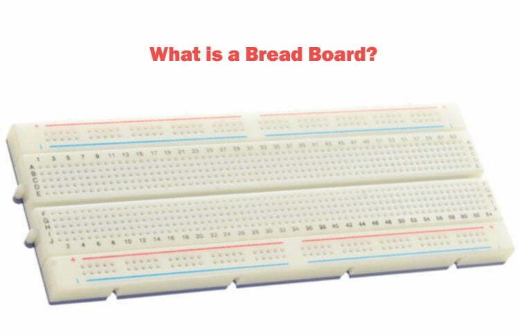
New to breadboards? Learn terminal strip layout, jumper wire connections, and component placement. Essential for circuit prototyping before PCB design. Beginner’s guide!

When an electric current is introduced to an inductor or something that can store magnetic energy, it will respond in different ways depending on the specific attributes of that device.
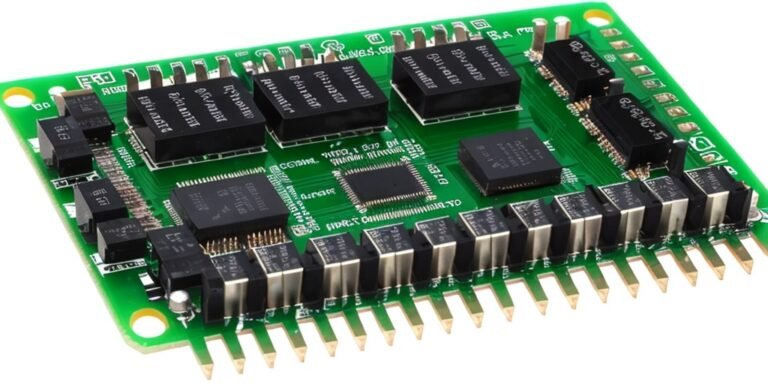
PIC18F14K50 Overview PIC18F14K50 is a low-cost microcontroller with advanced features and special value in the embedded USB market. It has a full-speed USB 2.0 compatible interface that can automatically change

What is a Counterbore? A counterbore, on the other hand, is a cylindrical hole with a flat bottom, typically consisting of two parts: a larger diameter top section and a
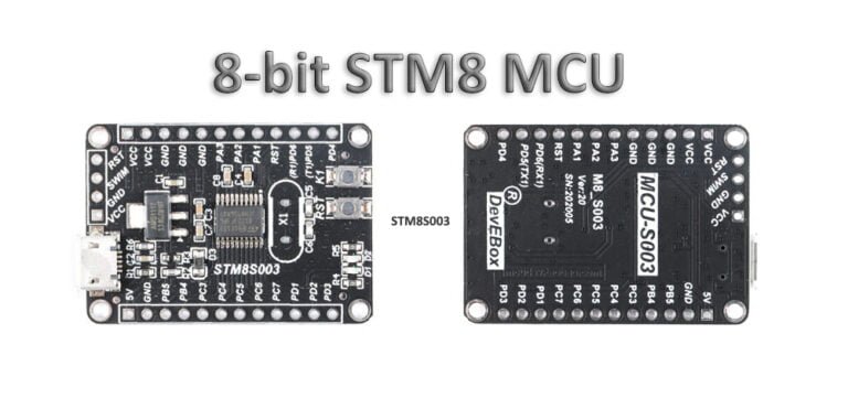
STM8 specs: 8-bit architecture, low-power modes, and ST Visual Develop setup. Learn GPIO, timers, and peripheral integration. Ideal for cost-effective designs!
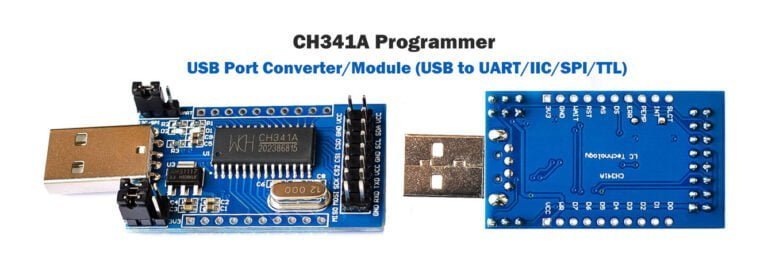
CH341A Programmer – USB Port Converter CH341A Programmer is a tool used for programming and reading data from various microcontrollers, EEPROMs, and other types of memory chips. It is a
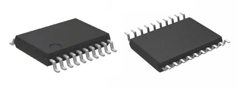
STM8S003F3P6TR Description STM8S003F3P6TR is a low-power, high-performance 8-bit microcontroller chip produced by STMicroelectronics. The chip adopts the core of STM8S series, and has various communication interfaces such as high-speed counter,
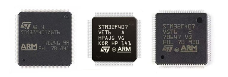
In the field of embedded systems, microcontrollers, as key components, play an important role in scenarios such as automatic control, Internet of Things, and industrial applications. The STM32F407 launched by

Introduction to Boolean expressions Boolean expressions are fundamental components of digital logic design. They represent logical relationships between variables, typically resulting in a binary output. These expressions are crucial for

Conduct flying probe tests: setup, coverage, and defect detection. Learn to validate prototype PCBs without fixtures. Tips for improving yield. Step-by-step inside!

The need for faster and more reliable electronic devices keeps growing. This makes high-frequency PCBs (Printed Circuit Boards) crucial in communication circuits. These PCBs work at frequencies above 1GHz. They