CH341A Programmer - USB Port Converter
CH341A Programmer is a tool used for programming and reading data from various microcontrollers, EEPROMs, and other types of memory chips. It is a small, portable device that connects to a computer via USB and can support a wide range of chips, making it a versatile tool for electronics enthusiasts and professionals alike. The CH341A Programmer is particularly useful for those working with embedded systems and microcontrollers as it allows for easy programming and debugging. It can be used to flash firmware, update settings, and transfer data to and from chips. Overall, the CH341A Programmer is an essential tool for those working in the field of electronics and programming.
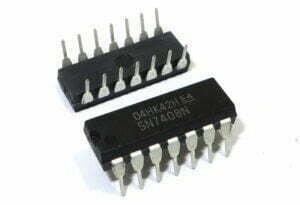
CH341A Chip Overview
CH341A is a USB bus convert chip, providing UART, printer port, parallel and synchronous serial with 2-wire or 4-wire through USB bus.

CH341A Features
- It adopts the classic WCH CH341A main control, which is fully compatible with the existing host computer.
- USB Type-C interface, A2C or C2C data cable can be easily extended, no longer bound.
- ZIF16 programming seat + 13Pin pin header, diversified interfaces support various target board requirements.
- Support 1.8/3.3/5.0V target device voltage, low-voltage chips do not need a level conversion board.
- Two modes of programming and serial port are optional, and online switching does not need to plug and unplug USB.
- Better current limiting protection function, improve on-board programming compatibility.
- Lightweight design, fairly sized U disk, easy to store and carry.
- Support 24 series EEPROM and 25 series SPI FLASH.
- IIC\SPI programming and USB to TTL mode switching.
- IIC\SPI programming is used with programming software.
- There are SOIC8, TSSOP8, TDFN8, DIP8 packages on the board.
- The interface leads out and can be connected to the burning folder.
- The serial port leads out and can be used as a USB-to-serial port.
- Supported OS Microsoft Windows (x86/x64), Linux (x86/x64/Arm), macOS (x86/Apple M1).
- Software Asprogrammer/NeoProgrammer (Windows GUI).
CH341A Parameters
- 5V, 3.3V power supply switching.
- USB powered 300 mA per rail.
- USB host interface USB2.0 (Full-Speed 12Mbps).
- USB Type-C Target interface DIP16.
- SPI/I²C UART ZIF type DIP16 IC.
- Test socket & 13Pin 0.1″.
- Terminal strips SPI/I²C UART.
- Serial baud rate 50bps – 2Mbps.
- Max programming speed 400kbps.
- Supported Target voltage 1.8V/3.3V/5.0V.
- Operating temperature -40 ~ 85℃.
- Relative humidity < 90 % rH.
- Board Size (without cables) 60.5mm x 25.5mm x 16mm.
- Weight 50g.
How to Burning the BIOS of a Motherboard Using CH341A?
Step 1: Confirm Pinout Order
This is a critical step as mistakes in this process can damage the motherboard. It is important to identify the correct pinout order for the BIOS chip and not to alter it once confirmed. The left eight pins in the figure below are for 25-series BIOS chips, while the right eight pins are for 24-series BIOS chips.
Step 2: Confirm Chip Voltage
To ensure the correct chip voltage, identify the chip model on the BIOS and look up its voltage requirements. For instance, the 25U12873F BIOS chip requires 1.8V, which requires the use of a voltage regulator board. The voltage regulator board has labeled pin numbers, with pin 4 as VCC and pin 8 as GND. If there are no labels, use a multimeter to measure the pins.
Step 3: Choose Programming Software
You can download the necessary drivers and C library from the WCH website. I highly recommend using NeoProgrammer, which is a reliable and professional chip programming software. Other software options are available, but if there is an issue with the programming device, only NeoProgrammer can identify it.
Step 4: Choose a Method to Program the Chip
There are three main methods to flash the BIOS chip:
- Disassembling and burning: For larger motherboards, you can remove the BIOS chip and burn it separately.
- Using SOP8 programming clip: This method is suitable for BIOS chips that are soldered onto the motherboard and cannot be removed. When using the clip, align the red line with the groove on the BIOS chip. Clamp one side first and then the other. Repeat this process until the software recognizes the chip.
- Using JSPI 1: Some motherboards come with an adapter socket that supports JSPI 1. You can purchase a JSPI 1 cable online. When burning the chip, align the white pin with the white corner on the JSPI 1 socket.
Step 5: Programming the BIOS Chip
5.1: Select Chip
In the programming software, select the correct chip model you are programming. Double check to make sure you have selected the correct chip, as programming the wrong chip can cause permanent damage to the device.
5.2: Detect Chip
Click the “Detect” button in the programming software to ensure that the chip is properly connected and detected by the programmer. If the chip is not detected, double-check the connections and try again.
5.3: Read Chip
Click the “Read” button to read the data from the chip. This is important to backup the existing data in case something goes wrong during programming.
5.4: Program Chip
Click the “Program” button to program the chip with the new data. This may take a few minutes depending on the size of the data.
5.5: Verify Chip
Click the “Verify” button to compare the programmed data with the original data read from the chip. This ensures that the data was programmed correctly and the chip is functioning properly.
Technical Application Notes for CH341A Programmer - Burning BIOS Chip
These additions address practical search intent while preserving the original page structure and existing ranking content.
- Check the key electrical, mechanical, and environmental assumptions before applying the page guidance to a real design.
- Cross-reference critical values with the latest datasheet, application note, IPC document, or manufacturer capability table.
- During PCB implementation, account for package size, thermal path, signal routing, power distribution, and test access.