System in a Package (SiP) technology has revolutionized the way electronic components are packaged and integrated into devices. SiP technology allows for more components to be integrated into a much smaller package, making it easier to design and manufacture smaller and more efficient electronic devices. In this blog post, I will discuss what System in a Package technology is, the benefits of SiP technology, the history of SiP technology, the overview of Octavo Systems’ SiP technology, the advantages of Octavo Systems’ SiP technology, applications of Octavo Systems’ SiP technology, trends in SiP technology, key players in the SiP technology market, and the future of SiP technology.
What is System in a Package (SiP) technology?
System in a Package (SiP) technology is a type of packaging technology that integrates multiple components into a single package. This type of technology is also known as system on package (SOP) or system on a package (SOAP). SiP technology is an evolution of traditional packaging technology, which typically consists of a single integrated circuit (IC) in a single package. SiP technology allows for multiple components to be integrated into a single package, reducing the size and increasing efficiency.
SiP technology offers several advantages over traditional packaging technology. It reduces the physical size of the package, allowing more components to be integrated into a smaller package. It also reduces the complexity of the design and manufacturing process, as fewer parts are needed to achieve the desired performance. Additionally, SiP technology improves signal integrity, as the package is more tightly integrated. This increases the speed and accuracy of communication between components, allowing for faster performance and more efficient data transfers.

Benefits of SiP technology
SiP technology offers a number of benefits over traditional packaging technology. The details are as below:
| Advantage | Description |
|---|---|
| High Electrical Performance | Multiple devices integrated in SiP systems reduce solder joints and improve electrical performance. |
| Low Power Consumption | SiP offers low power consumption and low noise system connections. |
| Low System Cost | Low power consumption and low noise design can result in cost savings compared to SoC. |
| Good Stability | Good resistance to drops and corrosion, high reliability, can be used in complex electromagnetic fields. |
| Short Product Launch | Simple design, reduced complexity and shorter implementation time compared to SoC. |
| Good Compatibility | Chips of different materials and processes can be combined in one system with embedded passive components. |
| Widely Used | Can handle digital and non-digital systems, including optical communication and sensors. |
| Small Physical Size | SiP packages becoming thinner, with advanced tech resulting in 1.0mm five-layer stacked chips. |
| High Packaging Efficiency | Multiple chips in one package, reducing peripheral circuit area and creating miniaturized, high-density substrates. |
History of SiP technology
SiP technology has been around since the early 2000s, when it was first used in the development of 3G and 4G cellular networks. At the time, SiP technology was seen as a way to reduce the physical size of the packages used to integrate components into devices. This allowed for more components to be integrated into a much smaller package, increasing device performance and efficiency.
Since then, SiP technology has seen a number of advancements. Most recently, SiP technology has been used in the development of 5G networks, where it has been used to reduce the size of packages and improve the speed and accuracy of communication between components. Additionally, SiP technology has been used in the development of automotive and aerospace components, where it has been used to reduce the size and complexity of packages.
SiP Packaging
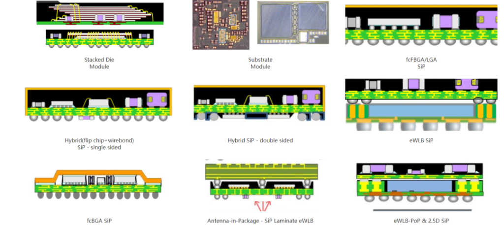
The dominant packaging forms of SiP include 2D flat multi-chip module (MCM) packaging, with forms such as Stacked Die Module, Substrate Module, FcFBGA/LGA SiP, Hybrid (flip chip+wirebond) SiP-single sided, Hybrid SiP-double sided, eWLB SiP, fcBGA SiP, etc. In 2.5D packaging, there are forms such as Antenna-in-Package-SiP Laminate eWLB, eWLB-PoP & 2.5D SiP. In 3D structures, chips are stacked directly and can be assembled using lead bonding, inverted chips, or a combination of both, or through silicon via technology for interconnection.

The components that make up SiP technology include packaging carriers and assembly processes. The former includes substrates, LTCC, and Silicon Submount (which can also be an IC). The latter includes traditional packaging processes (Wirebond and FlipChip) and JI and SMT equipment. Passive components are an important part of SiP, some of which can be integrated with the carrier (Embedded, MCM-D, etc.), while others (such as high-precision, high-Q, high-value inductors and capacitors) are assembled on the carrier through SMT. The dominant packaging form of SiP is BGA. Currently, there is no special technology or material for SiP itself. This does not mean that SiP technology is mastered by possessing traditional advanced packaging technology. Due to the industrial model of SiP no longer being single OEM, module division and circuit design are also important factors. Module division refers to separating a piece of functionality from an electronic device, which is convenient for subsequent system integration and SiP packaging.
Application of SiP Technology
SiP technology is used in a variety of applications, including automotive, aerospace, and consumer electronics. See details below:
| Application | Description |
|---|---|
| Automotive electronics | SiP technology is used in the engine control unit (ECU) of automotive electronics. The ECU consists of a microprocessor (CPU), memory (ROM, RAM), input/output interface (I/O), analog-to-digital converter (A/D), and other large-scale integrated circuits. Different chips are integrated together using the SiP method to form a complete control system. |
| Medical electronics | SiP technology is used in implantable electronic medical devices, such as capsule endoscopes. Capsule endoscopes consist of optical lenses, image processing chips, radio frequency signal transmitters, antennas, and batteries. |
| Computing | SiP technology is mainly used in the computer field by integrating processors and memory. |
| Consumer electronics | Includes image processing chips (ISP) and Bluetooth chips. |
| Bluetooth systems | Bluetooth systems typically consist of a wireless part, link control part, link management support part, and main terminal interface. SiP technology makes Bluetooth smaller and more market-friendly, thereby promoting its application. |
| Military electronics | Bluetooth systems typically consist of a wireless part, link control part, link management support part, and main terminal interface. SiP technology makes Bluetooth smaller and more market-friendly, thereby promoting its application. |
| Smartphones | RFPA is the most commonly used SiP form in smartphones. |
Octavo Systems’ SiP technology
Octavo Systems, a provider of advanced SiP technology, has developed a number of SiP packages for use in a variety of applications. Octavo Systems’ SiP technology integrates multiple components into a single package, reducing the size of the package and increasing the efficiency of the components. This technology is used in a variety of applications, including automotive, aerospace, and consumer electronics.
Octavo Systems’ SiP technology offers a number of advantages over traditional packaging technology. It reduces the size of the package, allowing for more components to be integrated into a smaller package. It also reduces the complexity of the design and manufacturing process, as fewer parts are needed to achieve the desired performance. Additionally, Octavo Systems’ SiP technology improves signal integrity, allowing for faster performance and more efficient data transfers.
Advantages of Octavo Systems’ SiP technology
Octavo Systems’ SiP technology offers a number of advantages over traditional packaging technology. It reduces the physical size of the package, allowing more components to be integrated into a smaller package. It also reduces the complexity of the design and manufacturing process, as fewer parts are needed to achieve the desired performance. Additionally, Octavo Systems’ SiP technology improves signal integrity, allowing for faster performance and more efficient data transfers.
Octavo Systems’ SiP technology also reduces power consumption, as fewer components are needed to achieve the desired performance. This is especially beneficial for battery-powered devices, as it can significantly extend battery life. Additionally, Octavo Systems’ SiP technology reduces cost, as fewer components are needed to achieve the desired performance.
Finally, Octavo Systems’ SiP technology is more reliable than traditional packaging technology, as it reduces the number of components needed to achieve the desired performance. This reduces the chances of failure due to faulty components, and increases the reliability of the device.
Future Trends of SiP technology
With the advent of the IoT era, continuous development and research are helping to bring SiP closer to SoC with lower costs, smaller volume requirements, smaller initial investments, and positive trends in system simplification. In addition, the push to create larger and larger single-chip SoCs is beginning to touch the bottlenecks of design validation and manufacturability, as having larger bare chips leads to greater chances of failure and more losses of silicon wafers.
From the IP perspective, SiP is an excellent future substitute for SoC, as they can integrate the latest standards and protocols without the need for ongoing longer and more expensive redesign phases. Furthermore, the SiP approach allows for faster and more energy-efficient communication and power transmission, which is another encouraging factor to consider when looking at the long-term prospects of SiP adoption and application.