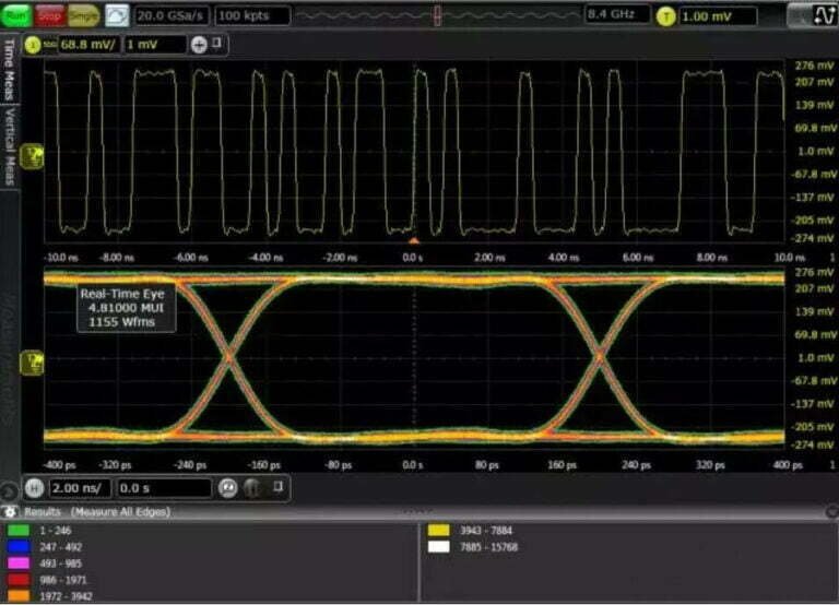
As the output switching speed of integrated circuits increases and the density of PCB boards increases, signal integrity has become one of the issues that must be concerned in high-speed digital PCB design. Because signal integrity problems may cause the system to output incorrect data, the circuit does not work properly or even completely Not working. So, how to fully consider the factor of signal integrity in the design process of PCB board and take effective control measures? Please read this article further.
What is PCB Signal Integrity?
The pcb signal integrity refers to the ability of the signal to respond with the correct timing and voltage in the circuit. It is a state where the signal is not damaged, and it indicates the quality of the signal on the signal line.
Different Signal Integrity Issues
Signal integrity problems can cause or directly bring about signal distortion, timing errors, incorrect data, address and control lines, system malfunction, and even system crashes. The main signal integrity problems include: delay, reflection, synchronous switching noise, oscillation , ground bounce, crosstalk, etc.
Delay
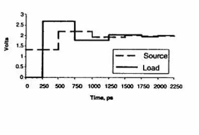
Delay means that the signal is transmitted at a limited speed on the wires of the PCB board, and the signal is sent from the sending end to the receiving end, and there is a transmission delay between them. The delay of the signal will affect the timing of the system, and the transmission delay mainly depends on the length of the wire and the dielectric constant of the medium around the wire. In a high-speed digital system, the length of the signal transmission line is the most direct factor affecting the clock pulse phase difference. The clock pulse phase difference means that the two clock signals generated at the same time are not synchronized when they arrive at the receiving end. The clock pulse phase difference reduces the predictability of signal edge arrival. If the clock pulse phase difference is too large, an erroneous signal will be generated at the receiving end. As shown in the figure below, the transmission line delay has become an important part of the clock pulse cycle.
Reflection
Reflection is the echo on the sub-transmission line. When the signal delay time is much longer than the signal transition time, the signal line must be regarded as a transmission line. When the characteristic impedance of the transmission line does not match the load impedance, part of the signal power (voltage or current) is transmitted on the line and reaches the load, but part is reflected. If the load impedance is less than the original impedance, the reflection is negative. Otherwise, the reflection is positive. Variations in routing geometry, improper transmission line termination, transmission through connectors, and discontinuities in power planes can cause such reflections.
Simultaneous Switching Noise (SSN)
The simultaneous switching noise will be generated, if many digital signals on the PCB are switched synchronously (such as CPU data bus, address bus, etc.). This is because there is impedance on the power line and ground, and there will be ground on the ground Plane bounce noise (ground bounce). The strength of SSN and ground bounce also depends on the I/O characteristics of the integrated circuit, the impedance of the PCB power layer and plane layer, and the layout and routing of high-speed devices on the PCB.
Crosstalk
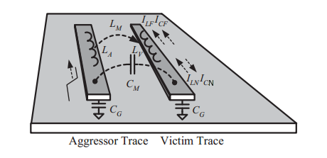
Crosstalk is the coupling between two signal lines, and the mutual inductance and mutual capacitance between the signal lines cause noise on the line. Capacitive coupling induces a coupled current while inductive coupling induces a coupled voltage. Crosstalk noise originates from electromagnetic coupling between signal nets, between signal systems and power distribution systems, and between vias. Cross-winding may cause false clocks, intermittent data errors, etc., and affect the transmission quality of adjacent signals. In fact, we don’t need to completely eliminate crosstalk, just keep it within the tolerance of the system. The parameters of the PCB board layer, the spacing of the signal lines, the electrical characteristics of the driver and receiver, and the baseline termination method all have a certain impact on crosstalk.
Overshoot and Undershoot
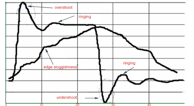
Overshoot is the first peak or valley exceeding the set voltage. For rising edges, it refers to the highest voltage, and for falling edges, it refers to the lowest voltage. Undershoot is when the next valley or peak exceeds the set voltage. Excessive overshoot can cause protection diodes to work, leading to their premature failure. Excessive undershoot can cause spurious clock or data errors (mishandling).
Ringing and Rounding
The oscillation phenomenon is repeated overshoot and undershoot. The oscillation of the signal is the oscillation caused by the transition inductance and capacitance on the line, which belongs to the underdamped state. The surround oscillation is an over-damped state. Oscillations and orbital oscillations, like reflections, are caused by a variety of factors. Oscillation can be reduced with proper termination, but it cannot be completely eliminated.
Ground Bounce Noise and Return Noise
Ground Bounce Noise
When there is a large current surge in the circuit, it will cause ground plane bounce noise. For example, if the outputs of a large number of chips are turned on at the same time, there will be a large transient current flowing through the power plane of the chip and the board. Power supply noise is then induced by the inductance and resistance of the chip package and the power plane, which creates voltage fluctuations and variations on the true ground plane (O V). This noise affects the operation of other components. An increase in load capacitance, a decrease in load resistance, an increase in ground inductance, and an increase in the number of switching devices will all lead to an increase in ground bounce.
Return Noise
Ground plane return noise is generated when digital signals travel to the analog ground area. This may be caused by the division of the ground plane (including power and ground), for example, the ground plane is divided into digital ground, analog ground, shield ground, etc. Likewise, power planes may also be split into 2.5 V, 3.3 V, 5 V, etc. Therefore, in multi-voltage PCB design, we need to pay special attention to the bounce noise and return noise of the ground plane.
Causes of Signal Integrity Issues
Factors such as the parameters of components and PCB boards, the layout of components on PCB boards, and the wiring of high-speed signal lines will cause signal integrity problems. For PCB layout, signal integrity needs to provide For circuit layout, signal integrity requires termination components, placement strategies, and routing information.
How to Optimize Signal Integrity?
The signal integrity problem is not caused by a single factor, but caused by multiple factors in the board-level design. Therefore, we need to use different methods to improve signal integrity according to specific situations.
Crosstalk analysis
The size of the crosstalk is inversely proportional to the line spacing, and proportional to the parallel length of the line and the signal frequency. Crosstalk will vary with circuit loading. For the same topology and wiring situation, the greater the load, the greater the crosstalk. In digital circuits, the edge change of the signal has the greatest impact on crosstalk, and the faster the edge changes, the greater the crosstalk. In view of the above characteristics of crosstalk, we can use the following methods to reduce crosstalk:
- Choose a slow device to reduce the transition rate of the signal edge;
- Avoid mixing different types of signals;
- Reduce coupling interference by reducing load;
- Minimize the parallel length between adjacent transmission lines;
- Increase the distance between conductors where capacitive coupling may occur;
- A more effective approach is to isolate the wires with ground wires;
- Insert a ground wire between adjacent signal wires;
- Minimize the number of loops and loop area;
- Avoid sharing the same wire for the signal loop;
- The signal layers of two adjacent layers should avoid parallel wiring as much as possible;
- Signals that are sensitive to crosstalk should be arranged in the inner layer as much as possible;
reflection analysis
Reflections occur whenever a signal encounters a change in impedance as it travels along a transmission line. The main way to solve the reflection problem is to perform termination impedance matching. There are usually two strategies for the termination of the transmission line: parallel termination and serial termination.
Parallel Termination
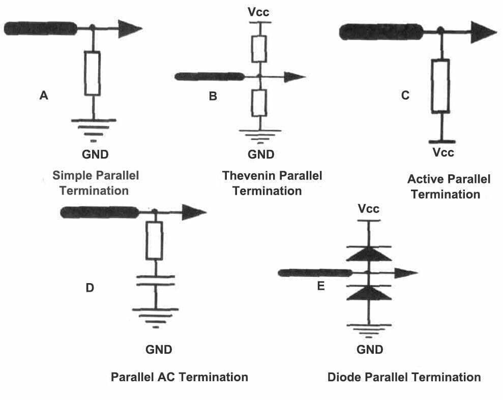
Parallel termination is mainly to connect the pull-up or pull-down impedance as close as possible to the load end to achieve impedance matching of the terminal. According to different application environments, parallel termination can be divided into several types as shown in the figure below.
Serial Termination
Serial termination is achieved by serially inserting a resistor into the transmission line as close as possible to the source. The serial termination is to match the impedance of the signal source, the resistance of the inserted serial resistor plus the output impedance of the driving source should be greater than or equal to the impedance of the transmission line. This strategy suppresses the signal reflected from the load by making the reflection coefficient of the source end zero (the input of the load end is high-impedance and does not absorb energy) and then reflects back to the load end from the source end.
Signal Integrity Analysis Modeling
Proper circuit modeling and simulation is the most common signal integrity solution. In high-speed circuit design, simulation analysis is increasingly showing superiority. Because it can provide designers with accurate and intuitive design results. In this way, we can detect problems early and correct them in time. There are three commonly used circuit modeling methods: SPICE model, IBIS model, and Verilog-A model.
SPICE model
SPICE is a powerful general-purpose analog circuit simulator. It consists of two parts: Model Equation and Model Parameters. Since the model equation is provided, the SPICE model can be very closely connected with the algorithm of the simulator, and better analysis efficiency and analysis results can be obtained.
IBIS model
The IBIS model is a model specially used for digital signal integrity analysis at PCB board level and system level. It uses the form of I/V and V/T tables to describe the characteristics of digital integrated circuit I/O cells and pins. The analysis accuracy of the IBIS model mainly depends on the number of data points and the accuracy of the data in the 1/V and V/T tables. Compared with the SPICE model, the calculation load of the IBIS model is very small.
Conclusion
With the continuous development of microelectronics technology, the use of high-speed devices and the design of high-speed digital systems are increasing. System data rates, clock rates, and circuit densities are also increasing. Therefore, the design requirements for the PCB board are getting higher and higher, especially the signal integrity issue. To ensure that the PCB has good signal integrity, a variety of influencing factors must be considered comprehensively.

