NPN transistors like the 2N2222 are commonly used for VHF amplifier and switching applications and are designed using silicon material. The 2N2222 transistor is considered a general-purpose transistor, so it is used like an NPN transistor and is primarily used as a small signal transistor.
The 2N2222A transistor is a common NPN BJI used primarily for low power switching and amplification applications, designed for low power, medium-low current, medium voltage, and high-speed operation.
2N2222A Transistor Overview
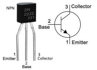
In the 2N2222 NPN transistor, a single P-doped layer is embedded between two N-doped layers. The transistor includes three terminals, such as the base, emitter, and collector, as shown in the figure below:
The 2N2222A transistor provides a constant DC collector current of 800mA and is therefore suitable for low to medium current applications. It operates at high conversion frequency values, such as 250MHz, with a 10ns delay time, 225ms storage time, 60ms fall time, and 25ms rise time and comes in a TO-92 package.
2N2222A Pin configuration
The pin configuration of the 2N2222A transistor includes three pins, and the functions of each pin are described below:

Pin1 (Collector): This is the first pin of the transistor, which is an o/p pin, and its main function is to provide transistor current to the o/p load.
Pin2 (Base): The base pin is the control pin, which is the second pin of the transistor, and its main function is to control the current from the emitter to the base.
Pin3 (Emitter): The emitter pin is the third pin of the transistor and is used to discharge all of the transistor’s current.
The configuration modes of the 2N2222 NPN transistor include common emitter (CE), common collector (CC), and common base (CB), which are very helpful for easily amplifying voltage, current, and power in different applications as required.
2N2222A Specifications
The specifications of the 2N2222A NPN transistor include the following:
| Parameter | Value |
|---|---|
| Transistor polarity | NPN |
| Terminal type | Through-hole |
| Pin configuration | a |
| Number of pins | 3 |
| Voltage between collector and emitter | 50V once the base is open |
| Voltage between emitter and base | 6V once the collector is open |
| Voltage between collector and base | 75V once the emitter is open |
| DC current gain | 100 |
| DC collector current | 800mA |
| Can be used in packaging | TO-92 |
| Total power dissipation | 1W |
| Maximum base current | 5mA |
| Input capacitance | 25pF |
| Output capacitance | 8pF |
| Fall time | 60ns |
| Rise time | 25ns |
- The complete power of the transistor should not exceed 500mW.
- The maximum handling frequency capacity is 250MHz.
- The maximum tolerance of its two terminals (such as base and collector) is 60V.
- For a collector current of 10mA and a voltage of 10V, the DC current is about 75mA.
Equivalent Alternative of 2N2222A
BC636, BC549, BC639, 2N2369, BC547, 2N3055, 2N3906, 2N3904, 2SC5200, 2N3904 (PNP), 2N2907 (PNP), 2N3906 (PNP), S9014, BC637, BC148, MPS2222, 2N4403, PN2222, KTN2222, and KN2222.
Circuit Diagram Example
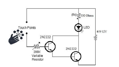
A touch switch circuit using a 2N2222A transistor is shown in the figure below. This simple circuit can also be used to connect any device or load to it through a relay to connect any device or load to operate through it.

The components required for this circuit include an input DC power supply of 6V, 2N1222 transistors – 2, resistors – 330Ω, 200KRΩ, and LED – 1.
This circuit can be built using two transistors (such as a Darlington pair), so the response time is very fast. It is also possible to add a timer circuit to extend the switch-on time, or to use a different type of switch, such as a touch sensor.
The first transistor amplifies the gain, which is then multiplied by the second transistor, resulting in high gain. Due to this high gain, this simple circuit is very sensitive to very small currents, making it useful for activating LEDs, for example.
The circuit can operate with 6V, 9V or 12V. If 6V is used, a 330Ω resistor must be used, while for 9V or 12V, a 390Ω/470Ω resistor must be used accordingly.
If a relay is used in place of the LED and resistors in the circuit, the same relay value must be used, as well as an adjustable 200KΩ resistor to adjust circuit sensitivity.
Once the contact point in the circuit is touched, a small amount of current is provided throughout the circuit to activate the LED.
Advantages and Disadvantages of the 2N2222A Transistor
Advantages:
- It is the most commonly used type of transistor.
- In electronic circuits, most switch applications can be accomplished using this transistor.
- Compared to other similar transistors, it is capable of handling relatively high current amplitudes.
- This transistor switches the load current with a current of up to 800mA, which is high compared to other transistors. Therefore, this feature makes the device an ideal choice for linear amplifier applications.
- Small size, lightweight, high voltage gain, low source voltage, low cost, and long lifespan.
Disadvantages:
- Highly sensitive and susceptible to temperature effects.
- Low input impedance.
- Small size makes it difficult to detect faults and challenging to replace.
- It does not work as effectively as relays or electrical/mechanical switches.
Applications of the 2N2222A Transistor
- Amplifying current.
- Switch to automatically turn on/off any electrical appliance.
- Due to its fast response time, it can be used for pulse width modulation.
- Typically used in automation and embedded projects.
- Audio preamplifier.
- Sensor circuits.
- Audio amplifier stage.
- Used to switch multiple loads simultaneously.
- Radio frequency circuits.
- Darlington pair.
- These transistors are used in motor drive circuits, such as variable frequency drives.
- Rectifier circuits and DC inverters.
- Amplifier to amplify voltage, current, and power.


