JFETs: Operation & Circuit Design Guide
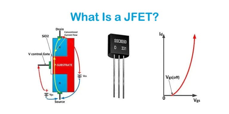
Junction Field-Effect Transistors: N-channel/P-channel basics, biasing, and advantages over MOSFETs. Ideal for low-noise amplifiers. Datasheet tips inside!
Junction Field-Effect Transistors: N-channel/P-channel basics, biasing, and advantages over MOSFETs. Ideal for low-noise amplifiers. Datasheet tips inside!

The real time clock design (RTC Design) is a chip that provides the correct date and time even when the power is off. It’s an essential component for IoT devices, industrial automation, and other applications where accurate timekeeping is essential.
Embedded systems design and development are driven by application requirements and IT technologies. With the continuous innovation and development of microelectronics technology, the integration level and process level of large-scale integrated circuits have been continuously improved. In particular, the introduction

Build PCB libraries: component footprints, symbols, and 3D models. Tools for Altium/KiCad and version control. Essential for efficient design. Tutorial inside!

/*! elementor – v3.9.1 – 14-12-2022 */ .elementor-heading-title{padding:0;margin:0;line-height:1}.elementor-widget-heading .elementor-heading-title[class*=elementor-size-]>a{color:inherit;font-size:inherit;line-height:inherit}.elementor-widget-heading .elementor-heading-title.elementor-size-small{font-size:15px}.elementor-widget-heading .elementor-heading-title.elementor-size-medium{font-size:19px}.elementor-widget-heading .elementor-heading-title.elementor-size-large{font-size:29px}.elementor-widget-heading .elementor-heading-title.elementor-size-xl{font-size:39px}.elementor-widget-heading .elementor-heading-title.elementor-size-xxl{font-size:59px} What is Solar PV Inverter? A solar PV inverter is an electrical device that converts the direct current (DC) electricity generated by solar panels into alternating
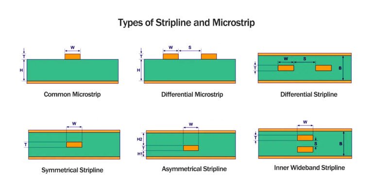
Explore the critical differences between stripline and microstrip with practical examples in 5G infrastructure, data centers, and medical devices. Optimize signal integrity for high-frequency PCB design.

Gerber files for PCBs: formats, layers, and why they’re critical for manufacturing. Learn to generate and verify files with Eagle/Altium. Step-by-step guide!
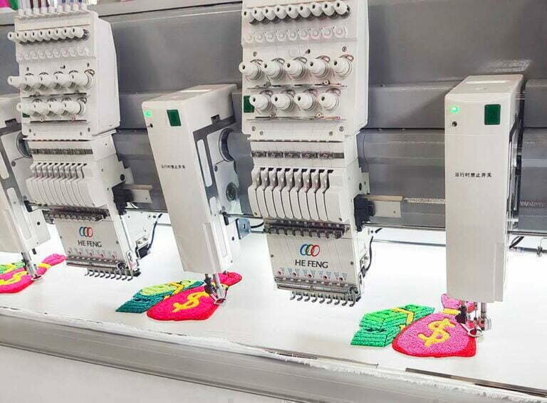
Embroidery Machine Introduction The embroidery machine can realize difficult and complex process, automatic head change, easy to operate. Widely used in various industries such as clothing, home textiles, curtains, children’s clothing, etc., with comprehensive functions to meet the requirements of
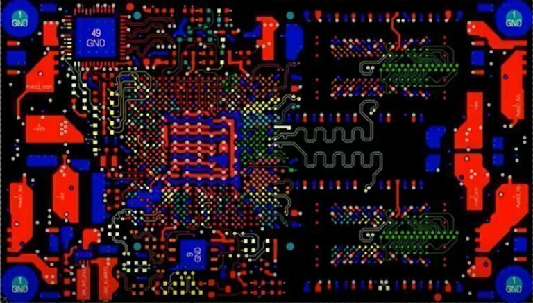
Design high-speed PCBs: impedance control, layer stacking, and crosstalk mitigation. Tools and strategies for 5G, USB 3.0, and HDMI layouts. Expert guide here!
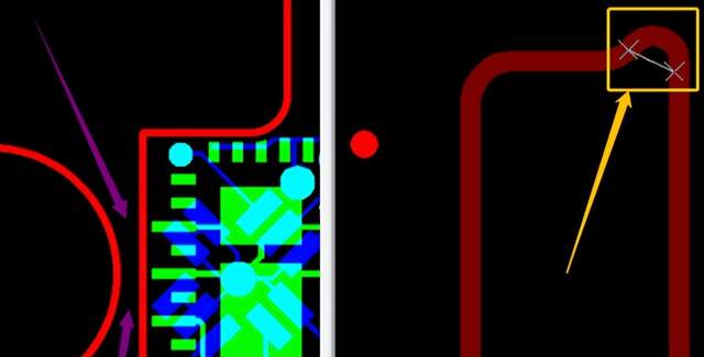
PCB Design Issues Drilling Hole Problem:Irregular hole ring design Risk:May confuse hole attributes Recommendation:Hole ring should be a hollow ring Problem:Holes without wire connections Risk:May lead to incorrect hole attributes Recommendation:Clearly define hole attributes in the source files Problem:Slot holes