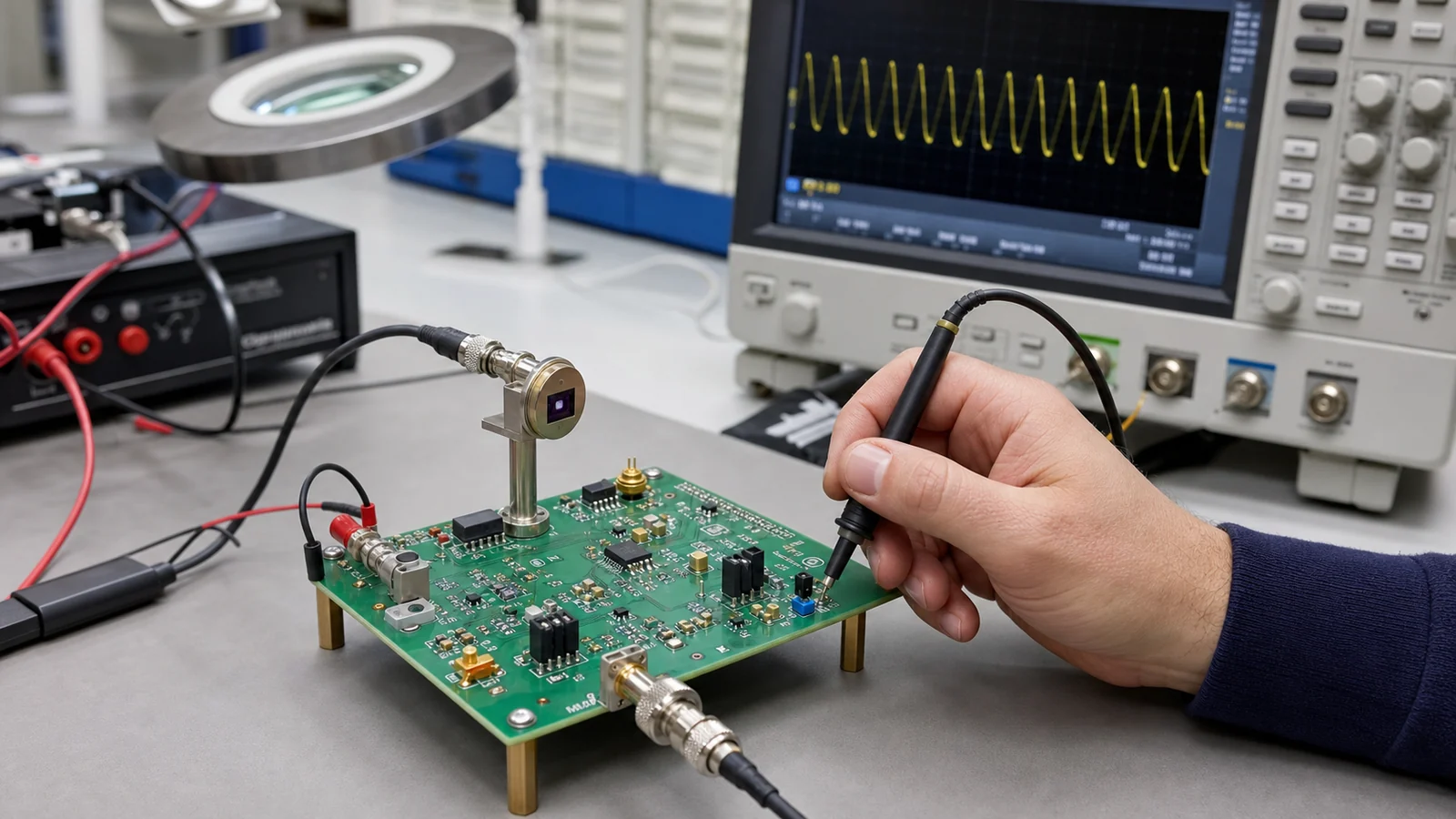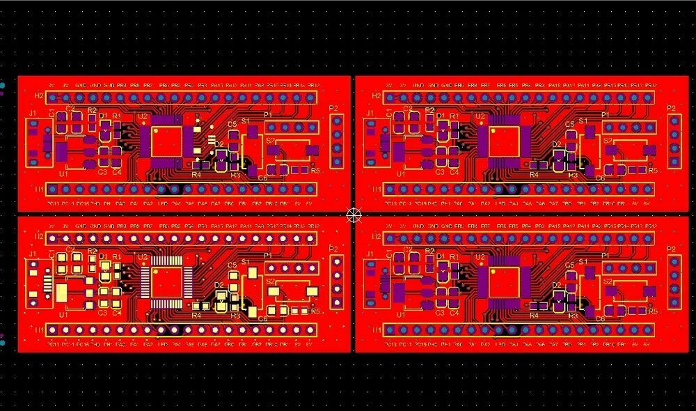
An impedance calculator can make a PCB look controlled long before the board is actually buildable. The number may say 50 ohms, but that result only stays useful if the copper thickness, dielectric height, solder mask, etch compensation, and launch geometry still match the real stackup that fabrication and assembly will deliver.
This guide explains how engineers should use a PCB impedance calculator without trusting it blindly. The useful question is not just which width reaches the target. It is whether the model still matches the coupon, the outer-layer finish, the via transition, and the release data that a board house will really build.
What a PCB Impedance Calculator Actually Solves
A calculator solves the straight-line geometry problem. It estimates trace width or spacing from the stackup, copper weight, dielectric constant, and target impedance. That is essential, especially for microstrip and stripline work, because guessing the width from a previous project usually fails once laminate height, copper thickness, or solder mask changes.
But the calculator only models the portion of the channel that behaves like the structure you entered. It does not validate connector launches, anti-pad shape, via stub length, skew through a differential escape, or whether the supplier will hit the dielectric and etch assumptions tightly enough to keep the result inside tolerance.
Why Calculator Results Drift When the Stackup Is Treated as a Placeholder
The fastest way to misuse an impedance calculator is to model against a provisional stackup and then forget to update the line when the board house proposes a different prepreg build. A small dielectric-height change can move the target width enough to matter. On tight-pitch routing, that shift may force a new escape strategy. On looser boards, it may quietly consume the impedance tolerance you thought you still had.
Solder mask and copper roughness also matter more than many layout reviews admit. Outer-layer lines do not see only air above the trace. They see mask thickness, resin content, and the final copper profile after fabrication. If the design review signs off a width using one assumption and production builds another, the calculator was never the problem. The stackup discipline was.
Use the Calculator Differently for Microstrip, Stripline, and Trace-Width Tradeoffs
Microstrip work is usually where engineers first notice model sensitivity because outer-layer traces are exposed to solder mask, finish variation, and fabrication tolerances more directly. Stripline is often more stable electrically, but it pushes different tradeoffs into layer count, lamination complexity, test access, and via planning. That is why the right question is not whether the calculator can hit 50 ohms in both structures. It is which structure still fits the routing density, cost target, and loss budget of the board.
If you need a refresher on that structural choice, ReversePCB’s stripline versus microstrip guide is useful background. The calculator belongs after that decision, not before it.
Where Trace-Width Calculators Stop Helping and Channel Geometry Takes Over
A trace-width or stripline impedance calculator does not tell you whether the connector launch is oversized, whether the BGA breakout forces a neck-down that destroys the local field shape, or whether a layer transition leaves too much via stub. Those failures do not show up in a single-width model, but they are often the first reason a real board rings, reflects, or misses eye margin.
That is why engineers should treat the calculator as the baseline geometry tool, then review every transition as a separate impedance event. A well-sized line feeding a poor launch is still a bad channel. If your signal-integrity debug keeps returning to the same connector or via field, the calculator has already done its job. The rest is layout and manufacturability.
How to Check Whether Your Calculator Inputs Are Trustworthy
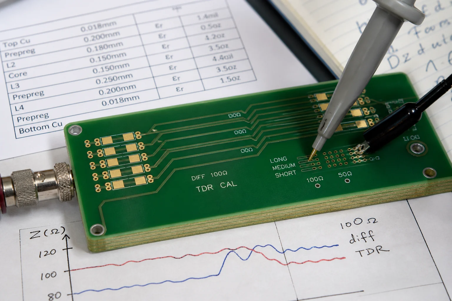
Before trusting the output, verify the actual inputs. Confirm the supplier’s intended dielectric build, finished copper thickness, and outer-layer treatment. Check whether the calculator expects finished or base copper, whether solder mask is included, and whether the dielectric constant matches the laminate family at the relevant frequency instead of a catalog placeholder. If your stackup note is still generic, the line result is generic too.
For teams moving from prototype to production, coupon strategy matters here as well. If the impedance coupon does not resemble the routing environment that matters, a passing coupon may still leave the product channel marginal. This is where DFM and SI stop being separate conversations.
What to Record Before Releasing an Impedance-Controlled Design
The release package should record more than a target number. It should lock the stackup intent, the trace class rules, the allowed tolerance, the coupon expectation, and any fabrication notes that affect the field environment above or around the line. If those assumptions live only inside one engineer’s calculator session, the board house and CAM team cannot reliably preserve them.
This is the same release-discipline problem described in ReversePCB’s Gerber release package guide. Controlled impedance is not just a routing rule. It is a documentation and manufacturing-control problem from the first quote to the final coupon review.
A Practical Review Checklist for Impedance Calculator Results
- Confirm that the stackup in the calculator matches the stackup the supplier will actually build.
- Check whether the model includes solder mask, finished copper assumptions, and the right dielectric family.
- Review neck-downs, via transitions, connector launches, and anti-pads separately from the straight-line width result.
- Align the calculated line with coupon planning, fabrication notes, and CAM release data.
- Revisit the model any time laminate height, copper weight, or outer-layer processing changes during quoting or DFM review.
A PCB impedance calculator is indispensable, but it is not a permission slip to stop thinking. Its value comes from tying geometry to a real stackup and then checking where the real board stops behaving like that idealized line. When that discipline is missing, the number is neat, but the hardware is still risky.
FAQ
What does a PCB impedance calculator actually calculate?
It calculates the straight-line relationship between target impedance and the line geometry allowed by a given stackup, such as width, spacing, copper thickness, and dielectric height. It does not validate every transition in the full channel.
Why can an impedance calculator result still fail on the real board?
Because connector launches, via stubs, neck-downs, solder mask assumptions, and stackup changes during fabrication can shift the real channel away from the modeled structure, even if the straight trace width was calculated correctly.
Is a stripline impedance calculator more reliable than a microstrip calculator?
Not automatically. Stripline geometry is often less exposed to outer-layer variation, but the right choice still depends on routing density, layer count, manufacturability, and loss budget. The calculator is only as reliable as the stackup and process assumptions behind it.
When should I recalculate PCB impedance?
Recalculate whenever the supplier changes dielectric build, copper weight, solder mask assumptions, or any outer-layer geometry that affects the field environment. Quote-stage stackups should never be treated as permanent by default.