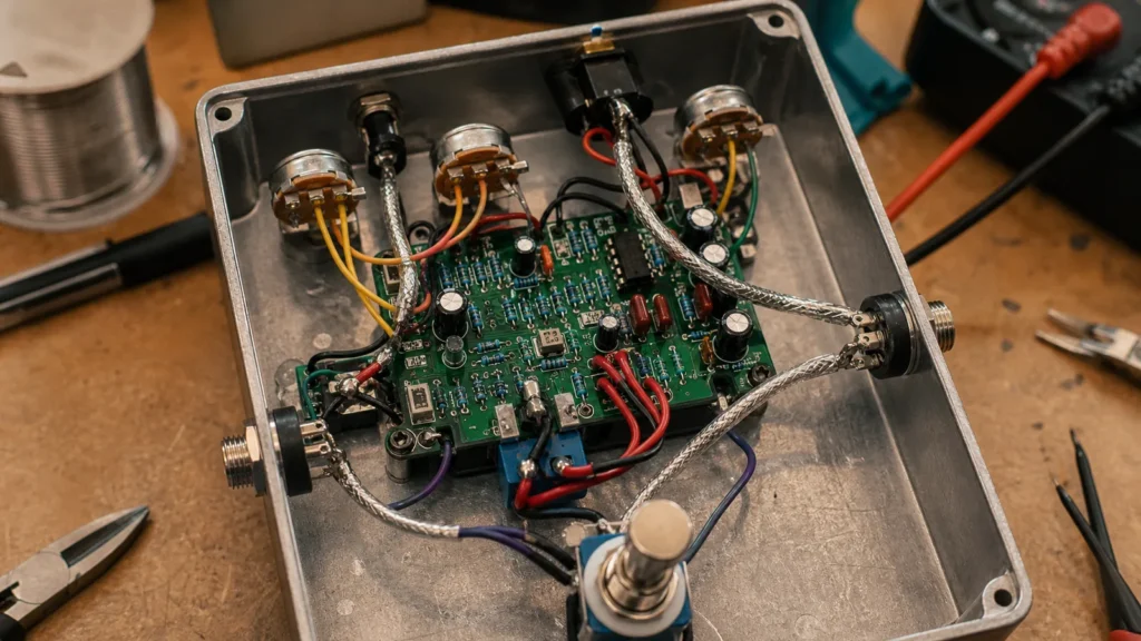
A guitar pedal PCB looks simple until a quiet bench prototype becomes a noisy, pop-prone, hard-to-service product. The keyword "guitar pedal pcb" usually points to more than a blank board for an effect circuit. Readers may be choosing a board for a DIY build, adapting a schematic to a stompbox enclosure, or trying to understand why one pedal behaves well while another hisses, ticks, or fails after repeated stage use.

In pedal work, the PCB sits at the intersection of electronics, mechanics, and user handling. Potentiometers, jacks, footswitches, LED wiring, battery or DC power inputs, and enclosure grounding all influence the final result. That is why a pedal board should be judged not only by whether the circuit fits, but by whether the layout supports clean audio, robust assembly, and practical repair.
Start with the signal path, not the artwork
Many pedal problems begin when layout follows enclosure convenience before signal flow. In an overdrive, fuzz, boost, or modulation effect, the quietest approach is to place the input network, bias references, active stages, tone shaping parts, and output driver in a logical sequence. Long meandering traces between gain stages increase the chance of oscillation and capacitive pickup. Tight routing around high-impedance nodes can also make the pedal more sensitive to hand proximity or switch wiring.
A good first pass is to split the board into functional zones: input conditioning, gain or filtering, switching and indication, and power conditioning. That same block-level thinking is useful when reading broader guides such as A Practical Way to Read Electrical Schematics for Circuit Work, because it helps you relate the symbol-level design to physical trace placement and debugging order.
Grounding is the real noise control system
In audio pedals, "ground" is rarely just one invisible node. The placement of returns determines whether charging current from an LED, bypass switching current, or a pulsing charge pump ends up modulating the signal reference. Designers often blame op-amps, transistors, or poor-quality parts when the larger fault is that the return path lets noisy currents share copper with the input or tone stack reference.
The practical rule is simple: keep the audio ground reference calm and keep higher-current returns predictable. The DC jack return, LED current return, relay coil return, and any switching converter ground should reach the main return without crossing the most sensitive signal reference areas. If you need a refresher on why return paths matter, the existing ReversePCB article on Ground in Electrical Circuits is worth linking directly because the same principle applies inside compact stompbox layouts.
Shielding by enclosure alone is not enough. The enclosure can help with interference, but it will not fix a layout that forces the input reference to ride on top of switching current. That is also why off-board wiring should be kept short and arranged deliberately. Twisted input and return wiring, controlled jack grounding, and thoughtful placement of the footswitch harness often do more than changing component brands.
Switching choices affect both tone and manufacturability
A pedal PCB is often judged by its bypass method. True bypass with a mechanical 3PDT footswitch is common because it is easy to understand and popular with builders. But it also adds wiring density, mechanical stress, and switching-pop risks. Buffered bypass, relay bypass, and soft-touch switching can improve user feel and reduce audio artifacts, but they demand clearer power sequencing and logic support.
From a PCB perspective, each switching method changes the board architecture. A true-bypass board may need better connector placement and clear silkscreen labels for switch lugs. A relay or soft-touch design needs clean control logic, debounce handling, and a current path that does not inject switching noise into the signal ground. A board that is easy to build by one hobbyist on a bench may become slow and error-prone in repeat assembly if the footswitch and jacks rely on awkward wire routing.
Power filtering should be treated as part of the audio design
Many pedal circuits are powered from a nominal 9 V supply, but that does not mean the power environment is gentle. Daisy-chained pedalboards, charge pumps, wall adapters, and reverse-polarity mistakes all show up in real use. The PCB should make room for reverse-polarity protection, local decoupling near active devices, and filtering that keeps supply ripple out of gain stages.
Charge-pump pedals deserve extra care because they create a new internal rail by switching current. That switching activity belongs away from the input and other high-gain nodes. If the pedal needs multiple rails or analog plus digital domains, the board partitioning should reflect that explicitly. This is the same design discipline discussed in general PCB layout guidelines for a successful design: keep noisy loops short, define return paths, and place decoupling where it actually works.
Mechanical fit is part of the electrical design
Guitar pedal PCBs fail mechanically in mundane ways. Pots may not line up with the enclosure, the DC jack may interfere with a tall capacitor, or the footswitch can flex the board if mounting support is weak. Builders often discover too late that a layout which looks fine in CAD becomes difficult to assemble once the stompbox hardware is installed.
That is why the enclosure drawing should be treated like a core design input. Confirm potentiometer spacing, threaded bushing reach, switch centerlines, battery clearance, and the distance from the board edge to the inside wall. If the pedal uses board-mounted jacks or footswitches, make sure the solder joints are not asked to carry all insertion or stomping force. Simple stand-offs or better connector selection can prevent cracked pads and intermittent faults.
Repair patterns are predictable if the board is documented well
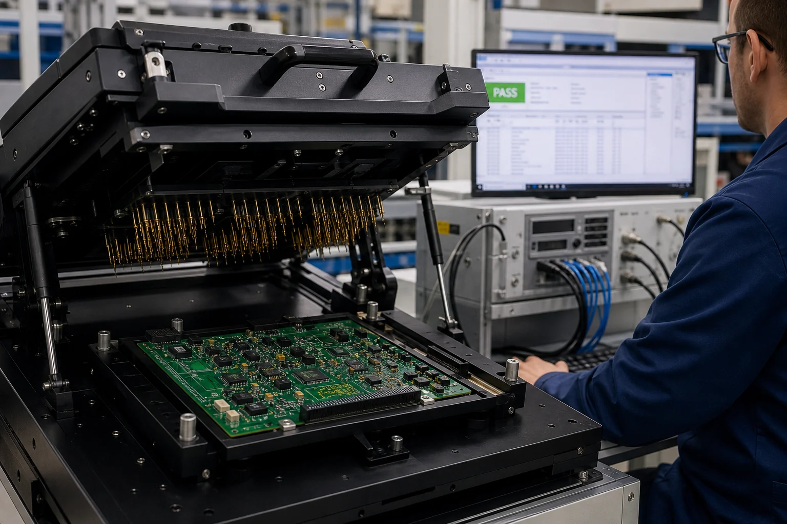
A repair technician approaching a guitar pedal PCB usually wants three things quickly: power integrity, signal path checkpoints, and confidence about off-board wiring. Boards become far easier to service when the silkscreen clearly marks transistor orientation, op-amp notch direction, pin 1 on ribbon headers, and testable supply rails. If the pedal uses a charge pump or switching controller, label that section clearly rather than treating it as background detail.
Common field issues include bypass popping, dead LEDs with otherwise working audio, oscillation when the gain is high, footswitch wear, lifted pads near jacks, and reverse-polarity damage. None of those faults become easier just because the schematic is available. The board has to expose test points and preserve enough physical access for probes and rework tools. A strong PCB repair workflow depends on layout choices made long before the first failure.
What to verify before fabrication
Before ordering or releasing a pedal PCB, verify five things. First, the grounding plan should be visible and intentional. Second, the switch and jack wiring should be easy to assemble without crossing the signal path unnecessarily. Third, the power entry should include the filtering and protection that matches how musicians actually power pedals. Fourth, enclosure alignment should be checked against real hardware dimensions, not assumptions. Fifth, the board should be serviceable: clear labels, probe access, and sensible part orientation all reduce future support cost.
If the board is moving beyond one-off DIY use, manufacturability matters even more. Clear polarity markers, stable footprints, and consistent assembly notes reduce build variation. ReversePCB's broader PCB assembly guidance applies here as well, especially when a design mixes through-hole mechanical parts with small-signal analog components that can be heat-sensitive or placement-sensitive.
Bottom line
A guitar pedal PCB is not just a carrier for an effect schematic. It is the practical structure that decides noise performance, switch feel, enclosure fit, assembly speed, and repair difficulty. The best pedal boards treat audio routing, ground strategy, power filtering, and mechanical packaging as one problem. When those details are handled early, the result is quieter on stage, faster to build, and much less painful to troubleshoot later.
Why are guitar pedal PCB layouts so sensitive to grounding?
Pedal circuits often handle small audio signals next to switching currents, LED indicators, and power conversion noise. Ground placement and return current routing can determine whether the pedal stays quiet or hums.
Is true bypass always better than buffered bypass?
Not automatically. True bypass is simple and popular, but a good buffer can preserve signal integrity in longer cable runs. The right choice depends on the pedal’s role in the chain and the switching scheme.
What should be checked before ordering a pedal PCB?
Confirm the enclosure size, potentiometer spacing, footswitch position, DC jack polarity, mounting holes, and whether the board keeps noisy power paths away from the audio section.
Can a pedal PCB be repaired if it pops when switching?
Often yes. The repair path usually starts with grounding, pulldown resistors, charge on coupling capacitors, switch wiring, and the power rail rather than replacing parts at random.