Do you hear about flash memory before? What is the difference between NOR and NAND? If you’ve been keeping tabs on the latest developments in computer hardware, you might have heard about these acronyms at least once. However, if you aren’t sure what they mean or how they work, this article is for you. Read on to find out more about these two different types of flash memory storage and how they work.
Flash Memory Definition
Flash memory is a type of non-volatile memory that can be erased and reprogrammed in blocks instead of one byte at a time. It’s generally used as storage media in digital cameras, handheld computers, MP3, USB flash drives and other small digital products. While flash memory is reprogrammable, other types of non-volatile memory, such as One-Time Programmable (OTP) memory, are designed for a single programming event.
Flash Memory Structure
Flash memory consists of an array of cells that can be individually programmed and erased. The cells can store a certain number of bits of data. Further more, each cell contains a floating-gate transistor with a control gate and a drain. The control gate controls the flow of electrons between the source and the drain. The floating gate stores the electrical charge, which represents the stored data.

How Flash Memory Work?
To explain the storage principle of flash memory, we still have to start with EPROM and EEPROM. Because flash memory combines the advantages of the high density of EPROM and the flexibility of EEPROM structure.
EPROM
EPROM means that the content in it can be erased by special means, and then rewritten. Its basic unit circuit is shown in the figure below. Floating gate avalanche injection MOS circuits are often used, referred to as FAMOS. It is similar to the MOS circuit. Two high-concentration P-type regions are grown on the N-type substrate, and the source S and drain D are respectively drawn out through ohmic contacts.

There is a polysilicon gate floating in the insulating layer between the source and the drain, and has no direct electrical connection with the surrounding. This circuit uses whether the floating gate is charged to indicate the storage of 1 or 0. When the floating gate is charged (such as a negative charge), a positive conductive channel is induced between the source and the drain, and the MOS transistor is turned on, which means that “0” is stored. If the floating gate is not charged, a conductive channel cannot be formed, and the MOS transistor is not turned on, that is, “1” is stored.
EEPROM
The working principle of the EEPROM basic storage unit circuit is shown in the figure below. Similar to EPROM, it regenerates a floating gate on top of the floating gate of the EPROM basic unit circuit. The former is called the first-level floating gate, and the latter is called the second-level floating gate. An electrode can be drawn out to the second-stage floating gate, so that the second-stage floating gate is connected to a voltage. If the voltage value is positive, a tunnel effect will occur between the first floating gate and the drain. This causes electrons to be injected into the first floating gate, ie programming. If the voltage value is negative, this will cause the electrons of the first floating gate to be lost, ie erased. The electrons can be rewritten after erasing.

Flash Memory
The basic unit circuit of flash memory is similar to EEPROM, and it is also composed of double-layer floating gate MOS transistors. But the first layer of gate dielectric is very thin, as a tunnel oxide layer.

The writing method of flash memory is the same as that of EEPROM, and a positive voltage is applied to the second-level floating gate to make electrons enter the first-level floating gate. Its reading method is the same as EPROM. In addition, the erasing method is to apply a positive voltage to the source and use the tunnel effect between the first-stage floating gate and the drain to attract the negative charges injected into the floating gate to the source.
When the electric field is withdrawn, connect 0V to the gate. If the MOS transistor is turned on, it is an erase cell, which is defined as logic “1”. If the MOS tube is not turned on, it is a program cell, which is defined as logic “0”. It is equivalent to “permanently” storing 1 bit of information in this unit. The magnitude of this threshold voltage is consistent with the number of electrons in the floating gate.
Since the positive voltage is applied to the source for erasing, the sources of each cell are connected together. In this way, erasure cannot be erased by byte, but erased in whole chip or block. With the improvement of semiconductor technology, flash memory has also realized a single-transistor design, mainly by adding floating gates and selection gates to the original transistors. When programming these memory devices, data is often organized in formats such as the HEX file format.
Flash Memory Cell
The magnitude of this threshold voltage is consistent with the number of electrons in the floating gate. According to the number of electrons injected into the floating gate, the cells of flash memory can be divided into several states:
SLC: single-level cell, 1bit, 2 states;
MLC: multi-level cell, 2 bits, 4 states;
TLC: tipple-level cell, 3 bits, 8 states;
QLC: Quad-level cell, 4 bits, 16 states.

Types of Flash Memory
Flash memory can be divided into two types: NOR flash and NAND flash. NOR flash allows for random access to individual cells, while NAND flash is typically used for mass storage devices, such as USB flash drives and memory cards.
NOR Flash
NOR flash memory is a “parallel” structure, and each cell has a separate word line and bit line. The characteristic of NOR Flash is to perform operations in the chip, so that the application program can run directly in the NOR Flash flash memory without having to read the code into the system RAM.

NAND flash
NAND flash memory is a “tandem” type structure, a string of flash memory cells are connected end to end, and they share a bit line. The basic storage unit of NAND flash memory is a “page”, similar to a sector of a hard disk. His advantage is that it can be made very small and highly integrated.

NOR Flash vs NAND Flash
NOR flash is more expensive than NAND flash, but it has a higher endurance and is more suitable for applications that require frequent read/write operations. NAND flash is cheaper and has a lower endurance, but it is faster and more suitable for applications that require large amounts of data storage.
History of Flash Memory
Compared to many short-lived information technologies, flash memory has a history of many years. In 1984, Toshiba first proposed the concept of fast flash memory. In the following decades, flash memory has undergone continuous iteration and development.
The First NOR Flash - 1988
Intel was the first company in the world to produce flash memory and put it on the market. In 1988, the company launched a 256K bit flash memory chip. It is embedded in a tape recorder. Later, this type of flash memory invented by Intel was collectively referred to as NOR flash memory. It combines two technologies of EPROM and EEPROM, and has a SRAM interface.
NAND Flash - 1989
The second type of flash memory is called NAND flash memory. It was developed by Hitachi in 1989 and was considered an ideal replacement for NOR flash memory. First of all, the write cycle of NAND flash memory is 90% shorter than that of NOR flash memory, and its storage and deletion speed is relatively fast. Secondly, the storage unit of NAND is only half of that of NOR, in a smaller storage space. Because of the excellent performance, the NAND is often applied to memory cards such as CompactFlash, SmartMedia, SD, MMC, xD, and PC cards, USB sticks, etc.
3D NAND flash - 2021
In 2021, China’s YMTC company released 128-layer 3D NAND flash memory. It has the highest storage density per unit area, the highest I/O transmission speed and the highest capacity of a single NAND flash memory chip.
Market of Flash Memory Devices
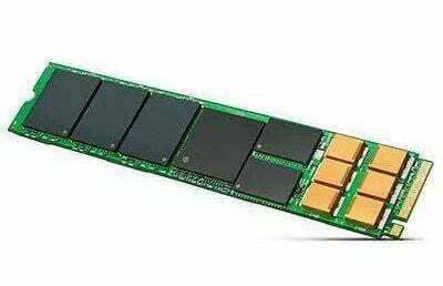
In the market, Samsung, Hitachi, Spansion and Intel are the four major manufacturers of flash memory devices. Among the flash memory devices, most people should be familiar with the flash memory hard disk. Compared with traditional hard disks, flash memory hard disks have high read and write speeds and low power consumption. In addition to flash drives, flash memory is also used in electronic products such as BIOS in computers, PDAs, digital cameras, voice recorders, mobile phones, digital TVs, and game consoles.
flash memory vs ssd
- Compared to SSD, the flash memory is smaller in size and lighter in quality;
- The flash memory structure is more resistant to falling than the SSD;
- Flash memory can provide faster data reading speed, while SSD is limited by rotational speed;
- Flash memory stores data more securely than SSD;
- Its non-mechanical structure, so movement will not affect its reading and writing;
- The life of flash memory is longer, while SSD is affected by the number of reads and writes and speed;
- SSD is written by magnetism, while the flash memory is written by voltage and the data will not be erased;
- The materials for making flash memory are scarce, so its unit storage capacity of flash memory is more expensive than SSD.
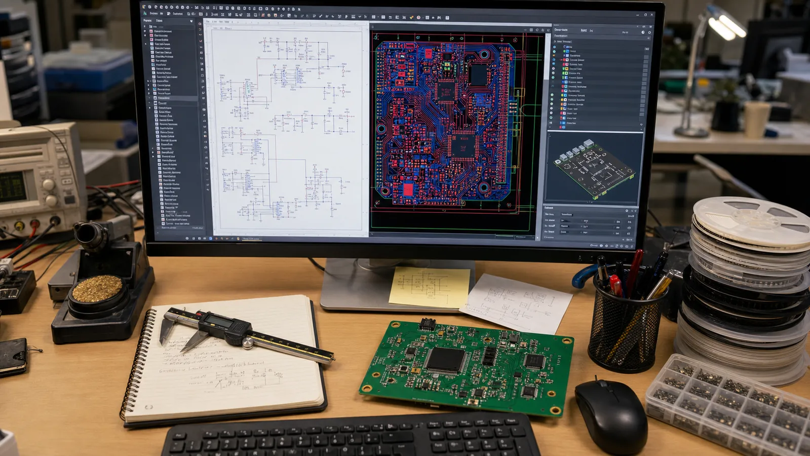
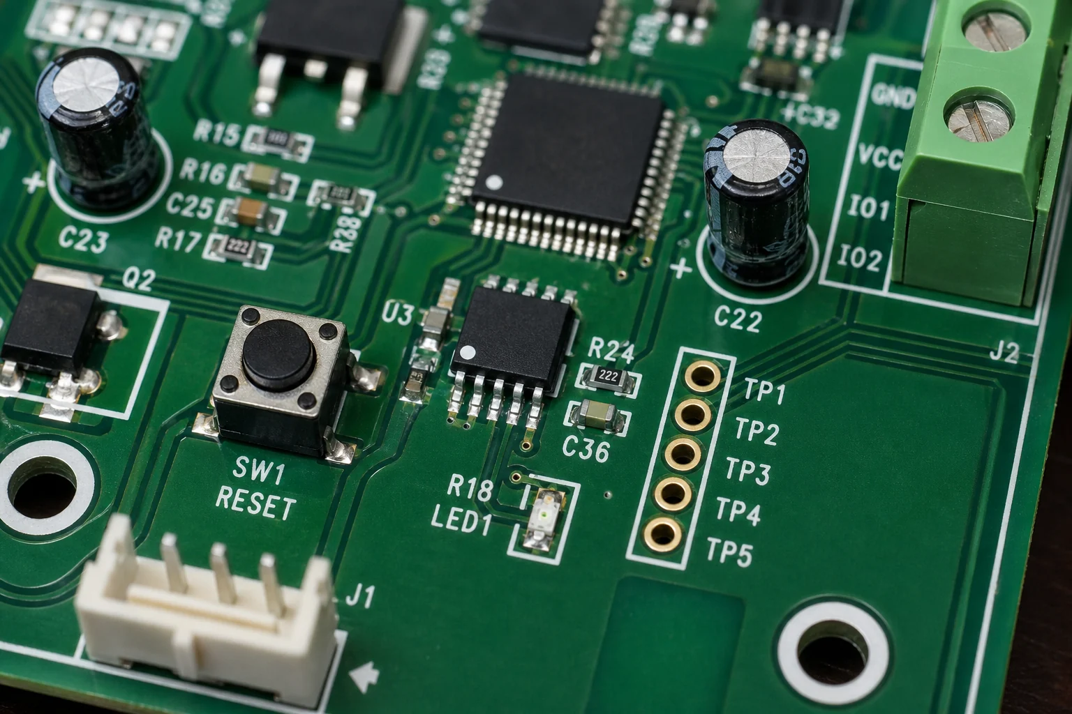
Engineering checks for Flash Memory Guide: Types & Applications
Before using Flash Memory Guide: Types & Applications in a PCB, firmware, repair, or validation workflow, confirm the details that usually decide whether the design works reliably instead of only reading the headline specification.
Design and troubleshooting checklist
| Area | What to check | Why it matters |
|---|---|---|
| Pinout and package | Verify the flash memory chips pinout, package variant, polarity, and footprint before assembly | Similar packages can have different pin order or exposed-pad rules |
| Electrical limits | Check voltage, current, power, frequency, thermal rating, and derating | Headline ratings rarely apply in every PCB condition |
| Substitution | Compare datasheets, markings, tolerances, and circuit role before replacing parts | Equivalent parts still need board-level evidence |
These checks help connect the search intent around flash memory chips with practical board-level decisions, component selection, and failure analysis.
Conclusion
In this blog, we introduce the flash memory of structure, development history, working methods and types. It has many features better than SSD. For most companies, flash memory remains a good investment despite the emergence of new alternatives such as MRAM and OUM in the market.
FAQ
All computer data can be stored, including files, programs, images, music, multimedia, etc.
The flash disk can be erased and written 1,000,000 times.
Just like all hard drives, the flash drives can be also infected by viruses.
A9 Windows98, Windows ME, Windows 2000, Windows XP, Windows7, Windows8, Windows8.1, MAC OS, Linux.