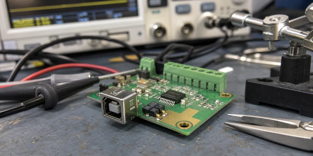
A TVS suppressor diode looks simple on the BOM, but it only protects a PCB when its voltage window, surge capability, and placement match the real fault path. Many boards still fail EFT, ESD, or cable-hot-plug events because the diode was chosen from a catalog table without checking connector location, cable energy, ground return inductance, or what the downstream IC can actually survive. This guide explains how to choose a TVS diode for power and I/O protection without turning a protection part into a leakage, capacitance, or false-pass problem.
What a TVS suppressor diode really does on a PCB
A TVS diode is not a magic surge absorber that makes any line safe. Its real job is to stay quiet during normal operation, then switch fast enough to divert transient current away from vulnerable silicon before the protected node exceeds a survivable level. In practice, that means the part has to be judged against the system, not against its package photo or peak-watt headline.
On a PCB, the important question is where the unwanted energy enters. A USB connector, 24 V field cable, motor lead, long sensor harness, or relay-driven node all create different surge shapes and different return-current paths. If the transient reaches the MCU pin, ADC front end, PHY, or DC/DC controller before the clamp sees a low-inductance path to ground, the TVS diode may be present and the board can still fail.
Start with the threat, not the part number
The fastest way to misapply a TVS diode is to begin with a distributor filter. Start by defining the event you are trying to survive: IEC-style ESD contact discharge, EFT bursts on a control cable, load-dump-like stress on a DC input, inductive kick from a local coil, or a hot-plug spike from a long harness. Those events differ in pulse width, source impedance, repetition, and where the energy returns.
For example, protecting a USB data pair is usually a capacitance and layout problem first, not a brute-force power problem. Protecting a 24 V industrial input is often a standoff-voltage and surge-energy problem. A relay or solenoid line may need the TVS diode to work with a flyback path instead of replacing it. If your prototype plan already includes cable stress and abuse cases, fold that work into PCB prototype first-build risk planning instead of treating protection as a last-minute patch.
The parameters that decide whether the TVS diode helps or hurts
The first number to check is reverse standoff voltage. It must stay above the highest normal operating voltage, including adapter tolerance, line overshoot, charger variation, and fault-free ringing. If that margin is too tight, the diode leaks, heats, or slowly corrupts measurements. This is common on 24 V nominal systems that briefly sit well above their nameplate voltage.
Next comes breakdown and clamp voltage. Those values only matter when compared with the absolute maximum rating and real survival margin of the protected device. A clamp that still lets the node rise above the transceiver, regulator, or ADC input limit is not real protection. On high-speed lines, junction capacitance matters just as much. A TVS diode that saves ESD but degrades eye margin, edge rate, or RF matching can move the failure from compliance testing to field performance.
Peak pulse power also needs context. Datasheet wattage is tied to a specific pulse shape, often much longer than the fast events that damage connector-facing electronics. Board designers should also check package size, thermal path, repetitive-stress behavior, and whether the source impedance in the real product is harsher than the marketing example. That is the same kind of package-selection tradeoff discussed when choosing surface-mount device packages: the package can change assembly yield, thermal behavior, inspection access, and reliability at the same time.
Placement and return path matter more than many BOM reviews expect
The TVS diode should sit at the entry point of the threat, not beside the IC you hope to protect. Put it as close as practical to the connector or cable landing point so the surge is diverted before it spreads across the board. The ground path must be short, wide, and tied into the return structure with as little loop inductance as possible. A long trace to a distant ground via often makes the clamp late enough to be ineffective.
This is where layout reviews often miss the real failure mode. The schematic can look correct, yet the current path forces transient energy through a long necked trace, a split return plane, or a via bottleneck before the diode conducts into a useful sink. In connectors that bring power and data together, it also helps to separate which lines need low-capacitance ESD arrays and which lines need higher-energy clamps. Treat the protection network as part of the current path, not as a symbol added after the fact. If the team needs a quick refresher on reading where those paths actually go, use this practical schematic-reading guide before layout review.
Where engineers get into trouble on real products
On USB and other fast I/O, the common mistake is choosing a rugged-looking TVS diode with too much capacitance or placing it behind a stub that adds discontinuity. On 24 V control inputs, the common mistake is selecting a low-voltage clamp that looks safe on paper but leaks during real supply tolerance or startup overshoot. On relay and solenoid lines, teams sometimes expect the TVS diode to solve every inductive event while forgetting contact bounce, ground bounce, and return-current injection into logic rails.
Another failure pattern shows up during repair. A board can pass low-energy bench pokes but still return from the field with damaged UARTs, Ethernet magnetics-side interfaces, sensor front ends, or power-input controllers because the original protection path was too far from the connector. In service work, a visibly intact TVS diode does not prove the design was correct. It may simply mean the transient found an easier path through the IC first.
How to validate a TVS diode design before release
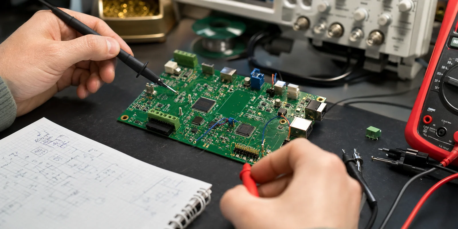
Validation should confirm both survival and behavior. The board still has to communicate, measure, boot, and recover correctly after the event. Run transient tests on the assembled PCB with the real connector, cable length, grounding method, and power state that the product will see. A bench-only test on a short loose wire often hides the inductance and coupling that create field failures.
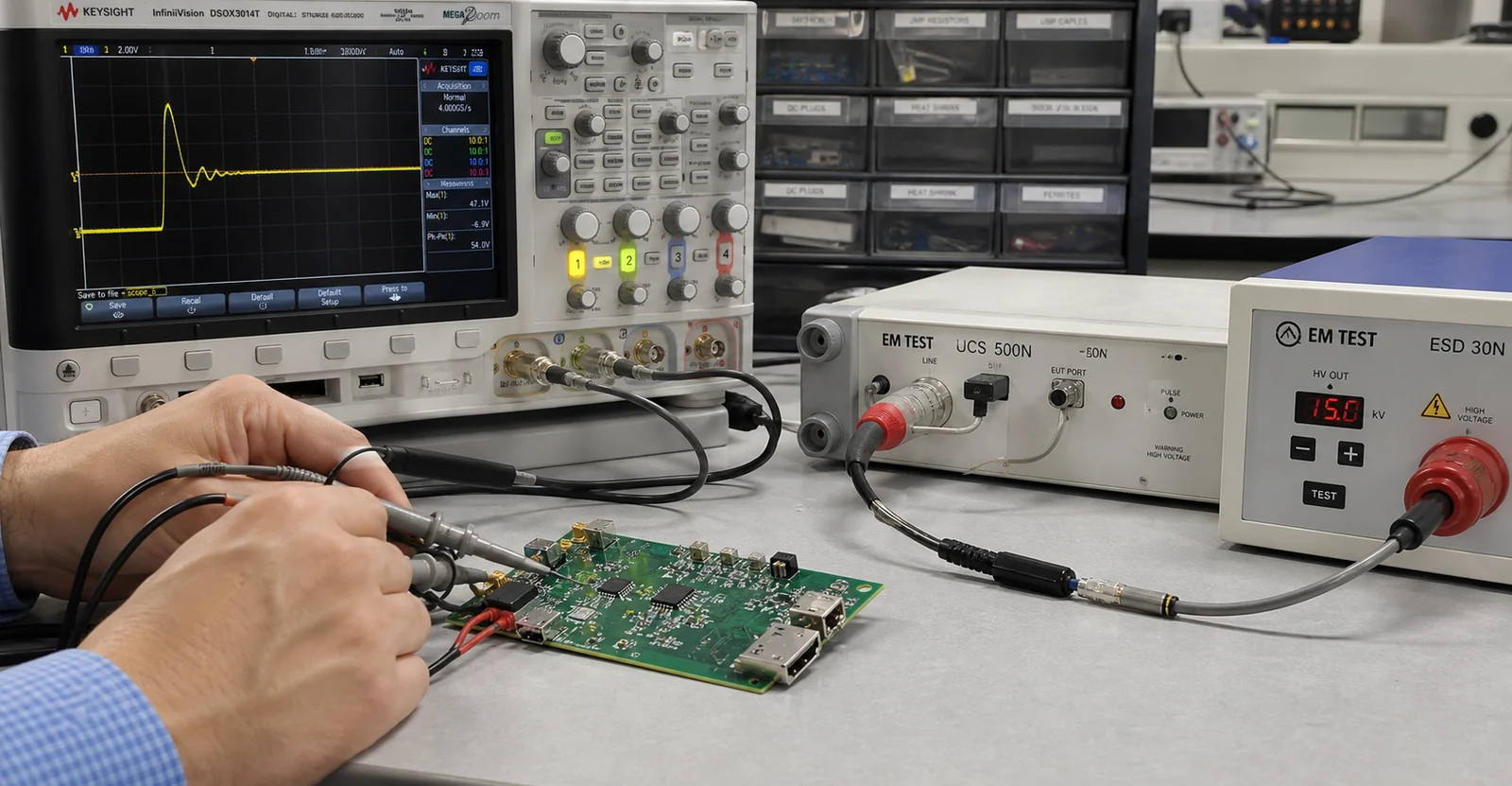
Use the oscilloscope to see what the protected node actually experiences, not just whether the power LED stays on. Check overshoot, ringing, clamp duration, and recovery behavior. If the protected interface talks to an MCU, watch for silent damage such as increased leakage, offset drift, intermittent resets, or corrupted communication after repeated hits. For boards exposed to residue, condensation, or contamination, verify that leakage and cleaning quality do not change the protection behavior in ways that confuse downstream circuitry.
When a TVS diode is not enough by itself
A TVS diode is often one layer in a protection strategy, not the whole strategy. Depending on the interface, the final network may also need series impedance, a common-mode choke, RC filtering, fuse coordination, flyback suppression, gas discharge or MOV stages, shielding, or connector pin sequencing. If the board uses conformal coating, potting, or sealing, check whether those decisions alter creepage, contamination trapping, or repairability around the protected entry point.
The best TVS diode choice is the one that matches the threat, protects the actual weak node, fits the layout, survives assembly and rework, and still lets the product behave normally. That is why a generic “TVS diode” answer is rarely enough. A TVS suppressor diode becomes valuable when it is chosen from the fault path backward, then proven on the assembled board under realistic stress.
FAQ
How do I choose the right TVS suppressor diode voltage for a PCB input?
Start with the highest normal operating voltage the line can see, including tolerance, startup overshoot, charger variation, and cable effects. Then choose a standoff voltage above that condition while confirming the clamp voltage still stays below what the protected IC can survive during the transient.
Where should a TVS diode be placed on a PCB?
Place it as close as practical to the connector or cable entry point, with a short low-inductance path into the return plane or chassis reference. Putting the diode beside the MCU or transceiver usually lets surge energy travel too far across the board first.
Can one TVS diode protect both power lines and high-speed data lines?
Usually no. Power inputs often need higher surge capability and can tolerate more capacitance, while USB, Ethernet, and other fast interfaces need low-capacitance protection that does not distort the signal. Mixed interfaces often need different protection parts on different lines.
Why can a board still fail ESD or surge testing even when a TVS diode is installed?
Common reasons include wrong standoff or clamp voltage, too much layout inductance, a long ground return, placing the diode away from the connector, or testing conditions that differ from the real cable and grounding setup. The part may be correct on paper but ineffective in the actual current path.