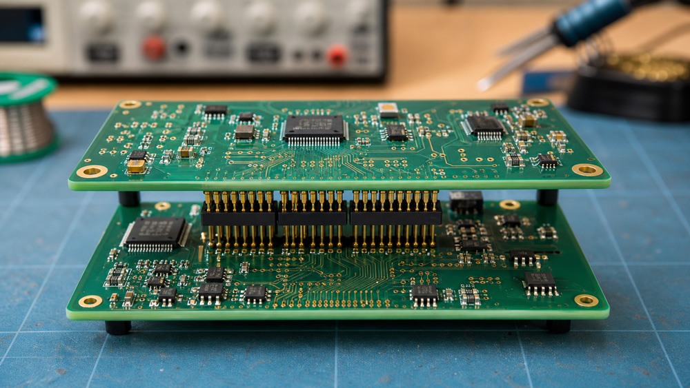
PCB on PCB is a practical way to describe one printed circuit board mounted, stacked, or connected to another printed circuit board. Engineers may also call this a board-to-board assembly, stacked PCB design, mezzanine board layout, daughterboard system, or module-on-board structure.
The idea is simple: instead of forcing every circuit onto one large board, you split the product into two or more boards that work together. One board may handle power and control, while another carries wireless communication, sensors, memory, displays, or a replaceable function module.
This guide explains how PCB on PCB designs work, where they make sense, what connection methods are used, and what design risks to check before production.
What Does PCB on PCB Mean?
PCB on PCB means one circuit board is mechanically and electrically connected to another circuit board. The boards may be stacked vertically, plugged together with connectors, soldered together through castellated pads, or linked with headers, sockets, flex cables, or interposers.
In many products, the lower board acts as the main board. The upper board may be a daughterboard, radio module, sensor board, display board, memory board, or power module. The exact structure depends on the product size, signal requirements, assembly process, and repair strategy.
The phrase is not always used as a formal industry term. In datasheets and manufacturing documents, you may see more specific names such as board-to-board connector assembly, mezzanine connector design, stacked PCB assembly, or multi-board system.
Why Use PCB on PCB Instead of One Larger Board?
PCB on PCB is useful when a product needs more circuit density, modularity, or design flexibility than one flat board can provide. It lets the design use vertical space instead of only increasing board length and width.
This is common in compact devices where the enclosure is tight. A handheld instrument, IoT gateway, medical device, camera module, or industrial controller may not have enough room for one large PCB. Stacking a smaller PCB above the main board can make the layout easier to fit.
It also helps when different functions need different design rules. For example, an RF module may need controlled impedance and careful antenna clearance, while the main board handles power, buttons, and lower-speed control signals. Separating those circuits can make the design cleaner.
PCB on PCB can also support product variants. A company may keep one base board and swap different daughterboards for Wi-Fi, Bluetooth, cellular, sensor, or regional interface options.
Common PCB on PCB Connection Methods
The connection method is the most important design choice in a PCB on PCB assembly. It affects signal quality, stack height, assembly cost, repairability, and long-term reliability.
PCB connectors are the cleanest option for many designs. They come in different pitches, heights, orientations, and pin counts. Some are made for compact consumer devices, while others are built for industrial vibration and repeated mating cycles.
Pin headers and sockets are simple and low-cost. They work well for prototypes, development boards, and low-speed signals. The tradeoff is size. They are usually taller and less compact than fine-pitch board-to-board connectors.
Castellated holes are common for small modules. A castellated module is soldered onto pads on the main PCB, almost like a surface-mount component. This approach is used for wireless modules, power modules, and sensor boards.
Flex or rigid-flex connections are useful when boards need to sit at an angle or move slightly during assembly. They can reduce connector height, but they add design and manufacturing complexity.
Key Design Rules for PCB on PCB Layout
A reliable PCB on PCB layout starts with mechanical alignment. The two boards must fit the enclosure, mate correctly, and avoid collisions with tall parts, shields, batteries, screws, heat sinks, or cables.
Check stack height early. Connector height, PCB thickness, solder joint height, component height, and enclosure clearance all add up. A design that looks fine in the schematic can fail mechanically if the boards sit too close together.
Plan the pinout before routing. Put ground pins near high-speed signals, keep power pins sized for current, and group related signals together. A poor connector pinout can make routing harder and increase noise.
Add test access. Once boards are stacked, some pads and components may be hidden. Test points, programming headers, and inspection access should be planned before the final layout.
Use mounting support where needed. Connectors alone may not be enough for products exposed to vibration, shock, or repeated handling. Standoffs, screws, guide pins, or mechanical brackets can reduce stress on solder joints.
Use proven PCB layout guidelines while checking stack height, connector placement, routing access, and test points.
Signal and Power Considerations
PCB on PCB designs need careful signal and power planning because current and data must pass between separate boards. The connector is not just a mechanical part; it becomes part of the electrical design.
For power, check current rating per pin and total connector heating. If the daughterboard draws high current, use multiple power and ground pins, wider traces, and enough copper area near the connector.
For high-speed signals, control return paths. A fast signal crossing from one board to another needs a nearby ground reference. Without a clean return path, the connector transition can create impedance changes, reflections, or EMI issues.
For analog signals, keep noisy digital or switching power lines away from sensitive pins. If the boards include sensors or audio circuits, pin assignment and grounding can make a noticeable difference.
For RF modules, follow the module vendor’s layout notes. Antenna clearance, ground keepouts, and nearby metal parts matter more than the connector alone.
Manufacturing and Assembly Risks
PCB on PCB assemblies are harder to build and inspect than a single flat PCB. The extra board, connector, solder joints, and alignment steps add more places where something can go wrong.
Connector placement tolerance is one risk. If mating connectors are slightly misaligned, the boards may not seat properly. This can lead to bent pins, intermittent signals, or mechanical stress.
Reflow compatibility is another issue. If both boards are assembled separately, the final joining method must not damage nearby components. If a daughterboard is soldered directly to the main board, the process needs a clear thermal plan.
Inspection can also be harder. Hidden solder joints, blocked test points, and tight spacing between boards make visual inspection more difficult. Design for inspection before the first prototype.
Repair strategy matters too. A plug-in daughterboard is easy to replace. A soldered module is more compact, but harder to remove without rework tools.
PCB on PCB vs Single PCB Design
A single PCB is usually simpler, cheaper, and easier to inspect. PCB on PCB becomes attractive when the product needs compact size, modular design, replaceable functions, or better separation between circuit blocks.
For simple products, one PCB is often the better choice. It reduces connectors, assembly steps, and mechanical risks. Fewer interconnects usually means fewer failure points.
For compact or modular products, PCB on PCB may be worth the extra complexity. It can reduce board area, simplify product variants, and let teams update one module without redesigning the entire board.
The decision should be made early. Moving from one PCB to stacked boards late in the project can affect the enclosure, BOM, routing, firmware testing, manufacturing flow, and service plan.
When PCB on PCB Is a Good Choice
PCB on PCB is a good choice when the design benefits from modularity, vertical space, or circuit separation. It is often used in IoT devices, embedded controllers, RF products, handheld tools, medical electronics, and industrial systems.
It is also useful when a design team wants to reuse an existing module. For example, a certified wireless module can be mounted on a custom base board, reducing RF design risk and shortening development time.
It may not be the best choice for very low-cost products, high-volume designs with tight assembly margins, or simple circuits that fit easily on one board. In those cases, a single PCB may be more reliable and easier to manufacture.
Conclusion
PCB on PCB design lets engineers connect multiple circuit boards into one compact system. It can save space, support modular products, and separate different circuit functions, but it also adds connector, alignment, signal, power, and inspection risks. Start by checking whether one PCB can do the job. If stacked boards make sense, plan the connector, stack height, pinout, test access, and mechanical support before layout begins. For a custom multi-board product, a PCB design service can help review the stackup, connector strategy, and manufacturing risks.