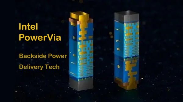
Not long ago, Intel achieved backside power delivery technology on a product-level test chip codenamed “Blue Sky Creek” to meet the performance demands of the next era of computing. Intel showcased the results of this research through two papers presented at the VLSI Symposium held in Kyoto, Japan, from June 11th to 16th of this year. More Info
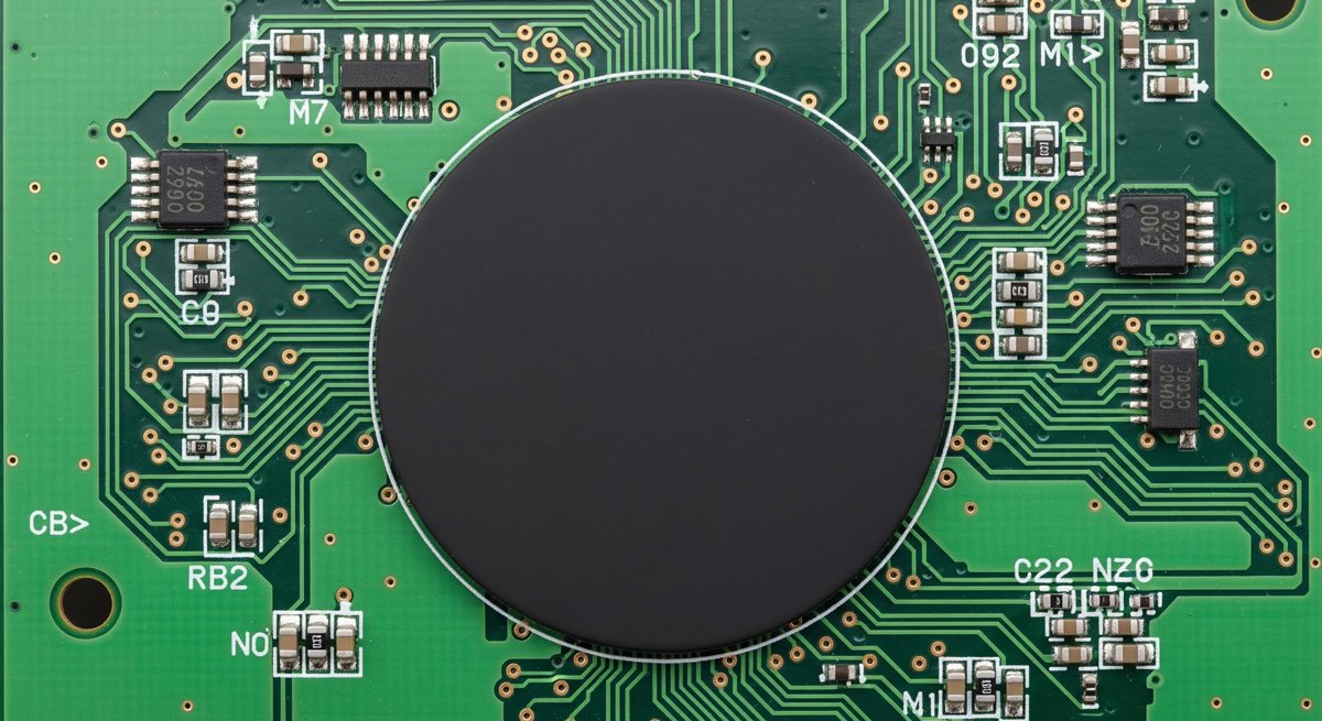
As the process nodes continue to advance, traditional front-side power delivery technology faces numerous challenges. With signal and power lines located on the front side of the wafer, they need to share or even compete for resources on each metal layer. This necessitates efforts to increase the spacing between metal layer pins, leading to higher costs and complexity. As a response, the industry has begun exploring the possibility of shifting power distribution to the backside. Backside power delivery technology separates signal and power lines, moving the latter to the backside of the wafer, enabling individual optimization. This brings about higher performance and lower costs, though it also presents challenges in terms of yield, reliability, heat dissipation, and debugging.

Reportedly, both the Intel 20A and Intel 18A process nodes will adopt the PowerVia backside power delivery technology along with the RibbonFET all-around gate technology. To address these challenges and expedite development, Intel chose to develop PowerVia and RibbonFET technologies separately, with PowerVia being the frontrunner. Through testing, PowerVia technology significantly enhances chip efficiency, with utilization rates exceeding 90% for most standard cell areas. Transistor sizes are notably reduced, unit density is greatly increased, and PowerVia achieves high yield and reliability indicators during testing, demonstrating the expected value of this technology. Testing also reveals that PowerVia reduces platform voltage by 30% and brings a 6% frequency gain.
In addition, Intel has developed heat dissipation technology to prevent overheating issues. The debugging team has also devised new techniques to address various issues that arise during debugging of this novel transistor design structure. PowerVia test chips display favorable heat dissipation characteristics, aligning with the expectations for achieving higher power density through logical miniaturization.

Ben Sell, Vice President of Technology Development at Intel, stated, “Intel is actively advancing the ‘Four Years, Five Process Nodes’ plan and is committed to integrating one trillion transistors in a single package by 2030. PowerVia represents a significant milestone for both of these goals. By adopting experimentally produced process nodes and their test chips, Intel has reduced the risk of applying backside power delivery to advanced process nodes and is bringing backside power delivery technology to the market.”
It is understood that in an upcoming third paper to be presented at the VLSI Symposium, Intel’s technical expert Mauro Kobrinsky will elaborate on Intel’s research achievements in more advanced deployment methods for PowerVia, such as simultaneous signal transmission and power delivery on both the front and back sides of the wafer.