MSP430F169 Overview
The MSP430F169 Microcontroller is one of the Texas Instruments MSP430 family. It comprises multiple devices that feature distinct sets of peripherals designed for diverse applications. The architecture of these microcontrollers, coupled with five low power modes, has been fine-tuned to optimize extended battery life for portable measurement applications. Moreover, the digitally controlled oscillator (DCO) enables quick wake-up times of less than 6 µs from low-power modes to active mode.
These microcontrollers find typical applications in sensor systems, industrial control applications, hand-held meters, and other similar domains.
Features
- Low power consumption;
- Five power-saving modes;
- Three-channel internal DMA;
- Serial onboard programming;
- Programmable code protection by security fuse;
- With brownout detector and bootstrap loader;
- Supply voltage monitor with programmable level detection.
Pinout Configuration
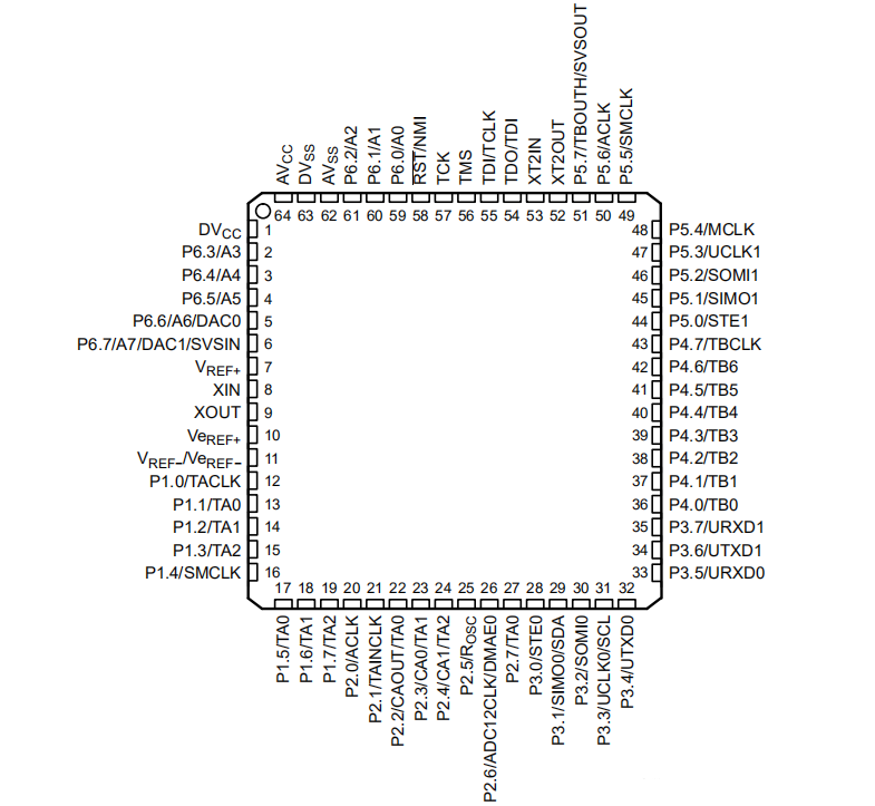
The MSP430F169 is actually available in both 64-pin and 100-pin versions, with different pin configurations for each.
For the 64-pin version, some key pins include:
| Pin Types | Pin Name | Description |
|---|---|---|
| Power Supply Pins | VCC | Positive supply voltage input |
| GND | Ground | |
| RST/NMI | Reset input and non-maskable interrupt | |
| TEST | Test mode input/output | |
| AVSS/AVCC | Ground and voltage reference for ADC | |
| DVSS/DVCC | Ground and voltage reference for digital circuitry | |
| Input/Output Pins | P1.x-P8.x | General-purpose I/O pins |
| Communication Pins | UCA0CLK | USART module A0 clock input/output |
| UCA0STE | USART module A0 STE input/output | |
| UCA0TXD | USART module A0 transmit data output | |
| UCA0RXD | USART module A0 receive data input | |
| UCB0CLK | SPI module B0 clock input/output | |
| UCB0STE | SPI module B0 STE input/output | |
| UCB0SIMO | SPI module B0 transmit data output | |
| UCB0SOMI | SPI module B0 receive data input | |
| UCB0SDA | I2C module B0 data input/output | |
| UCB0SCL | I2C module B0 clock input/output | |
| Timers and Counters | TA0CCR0-TA0CCR6 | Timer A0 capture/compare register 0-6 |
| Timer A0 control register | ||
| TB0CCR0-TB0CCR2 | Timer B0 capture/compare register 0-2 | |
| Timer B0 control register | ||
| Analog Pins | ADC12CLK | ADC12 clock input |
| ADC12MEM0-ADC12MEM15 | ADC12 memory register 0-15 | |
| AVREF+ | Positive reference voltage input for ADC | |
| AVREF- | Negative reference voltage input for ADC | |
| JTAG Pins | TCLK | Test clock input/output |
| TDI | Test data input | |
| TDO | Test data output | |
| Special Function Pins | ACLK | 32.768 kHz crystal oscillator input |
| SMCLK | System master clock output | |
| RTCCLK | Real-time clock input/output |
Specification
| Specification | Value |
|---|---|
| CPU | 16-bit RISC |
| Frequency | 8 MHz |
| Flash memory | 16 KB |
| RAM | 2 KB |
| Standby power | 1.1 µA |
| Active power | 330 µA at 1 MHz, 2.2 V |
| Wake-up time | in less than 6 µs |
| Instruction cycle time | 125 ns |
| Supply voltage | 1.8 V to 3.6 V |
| A/D converter | 12-bit |
| Timer/Counter | 2 * 16-bit |
| Operating Temp | -40 to 85 ℃ |
| DMA | 3 |
| I2C | 1 |
| SPI | 2 |
| Peripherals | timers, serial ports, I2C |
| Package | 64-pin QFP or 64-pin QFN |
Clock System of MSP430F169
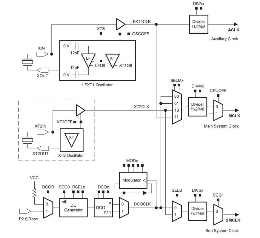
The clock system is very important to the single-chip microcomputer. The reason why the MSP430F169 single-chip microcomputer has such a low power consumption is because it has a powerful clock system!
Three clock signal sources
1. Low frequency LFXT1CLK (32.768KHz)
Standard crystal oscillator, oscillator or external clock source can be used to input 4MHz~32MHz. XT1CLK can be used as a reference clock for the internal FLL module.
The low-frequency crystal oscillator (32.768KHz) is directly connected to the single-chip microcomputer through the XIN and XOUT pins, and no other external devices are required (there is a 12pF load capacitance inside). At this time, the LFXT1 oscillator works in low frequency mode (XTS=0).
If the MCU is connected with a high-speed bulk oscillator or resonator, 0SCOFF=0 can make the LFXT1 oscillator work in high-frequency mode (XTS=1). At this time, the high-speed crystal oscillator or resonator is connected through the XIN and XOUT pins, and an external capacitor is required. The size of the capacitor is selected according to the characteristics of the crystal oscillator or resonator.
If the LFXT1CLK signal is not used as the SMCLK or MCIK signal, the software can set OSCOFF=1 to disable the LFXT1 from working, thereby reducing the power consumption of the microcontroller.
BCSCTL1:
XTS(BIT6)——LFXT1 high/low speed mode selection. 0: LFXT1 works in low-speed crystal oscillator mode (default); 1: LFXT1 works in high-speed crystal oscillator mode.
2. High frequency XT2CLK (8MHz)
Standard crystal oscillator, oscillator or external clock source can be used to input 4MHz~32MHz.
The XT2 oscillator generates the XT2CLK clock signal, and its working characteristics are similar to those of the LFXT1 oscillator when it works in high frequency mode. If XT2CLK is not used as the MCLK and SMCLK clock signal, the XT2 oscillator can be disabled with control bit XT2OFF.
BCSCTL1:
XT2OFF (BIT7) – XT2 high-speed crystal oscillator control. 0: XT2 high-speed crystal oscillator on; 1: XT2 high-speed crystal oscillator off.
3. Internal oscillator DCOCLK (1MHz)
Stabilized by the FLL module.
When the oscillator fails, DCO will be automatically selected as the clock source for MCLK.
The frequency of the DCO oscillator can be adjusted by software setting the DCOx. MODx and RSEL.x bits. When the DCOCLK signal is not used as the SMCLK and MCLK clock signal, the DC generator can be disabled with the control bit SCGO.
After the PUC signal, DCOCLK is automatically selected as the MCLK clock signal, and the clock source of MCLK can be additionally set to LFXT1 or XT2 as required. The setup sequence is as follows:
- Let OSCOFF=1;
- Let OFIFG=0;
- Delay and wait at least 50ps;
- Check OFIFG again, if OFIFG=1, repeat steps (3) and (4) until OFIFG=0.
DCOCTL:
DCOx (BIT7, BIT6, BIT5)——DCO frequency selection, 8 kinds of frequencies can be selected, and the DCOCLK frequency can be adjusted in sections. The frequency selection is based on the frequency band selected by RSELx. The relationship between DCOx, RSELx and the internal clock is as follows:
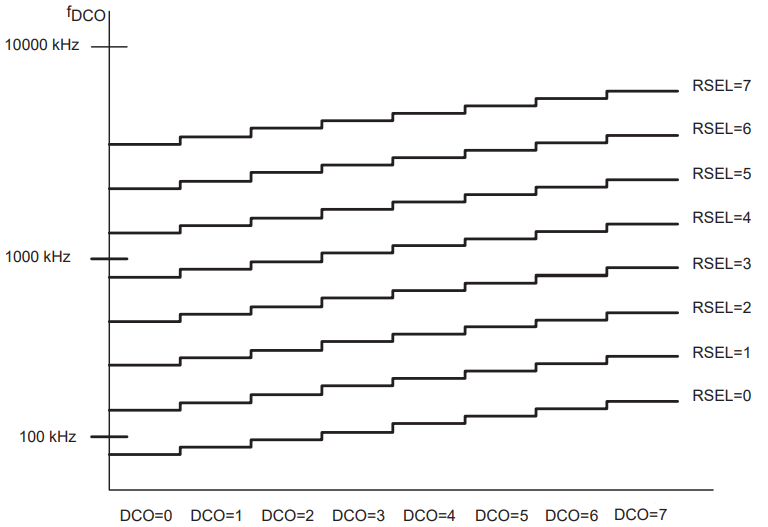
MODx (BIT4, BIT3, BIT2, BIT1, BIT0) – DAC modulator setting. The control switches the two frequencies selected by DCOx and DCOx+1 to fine-tune the output frequency of the DCO. If the DCOx constant is 7, it means that the highest frequency has been selected. At this time, MODx is invalid and cannot be used for frequency adjustment.
BCSCTL1:
RSELx (BIT2, BIT1, BIT0) – the frequency band selection of the DCO oscillator, these 3 bits control an internal resistance to determine the nominal frequency. 0: Select the lowest nominal frequency… 7: Select the highest nominal frequency.
BCSCTL2:
DCOR(BIT0)——Select DCO oscillator resistance. 0: internal resistance; 1: external resistance.
Three clock sources
1. ACLK auxiliary clock
ACLK is obtained after LFXT1CLK is divided by 1, 2, 4, and 8. It can be used as the clock signal of each peripheral module and is generally used for low-speed peripherals.
BCSCTL1:
DIVAx (BIT5, BIT4)——ACLK frequency division selection, the frequency division selection relationship is as follows:
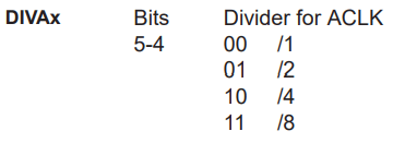
Macro definition: DIVA_0 (1 frequency division/no frequency division), DIVA_1 (2 frequency division), DIVA_2 (4 frequency division), DIVA_3 (8 frequency division)
2. MCLK system main clock
MCLK can be obtained from LFXT1CLK, XT2CLK, and DCOCLK after frequency division by 1, 2, 4, and 8. It is often used for CPU operation, program execution, and other modules that use high-speed clocks.
BCSCTL2:
SELMx (BIT7, BIT6) – select the MCLK clock source, the clock selection relationship is as follows:

Macro definition: SELM_0 (DCOCLK default), SELM_1 (DCOCLK), SELM_2 (XT2CLK), SELM_3 (LFXT1CLK)
DIVMx (BIT5, BIT4) – MCLK frequency division selection, the frequency division selection relationship is as follows:
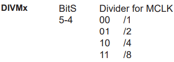
Macro definition: DIVM_0 (1 frequency division/no frequency division), DIVM_1 (2 frequency division), DIVM_2 (4 frequency division), DIVM_3 (8 frequency division)
3. SMCLK subsystem clock
SMCLK can be obtained by frequency division of XT2CLK and DCOCLK by 1, 2, 4, and 8, and is often used in high-speed peripheral modules.
BCSCTL2:
SELSx (BIT3) – select the MCLK clock source, the clock selection relationship is as follows:

DIVSx (BIT2, BIT1) – SMCLK frequency division selection, the frequency division selection relationship is as follows:

Macro definition: DIVS_0 (1 frequency division/no frequency division), DIVS_1 (2 frequency division), DIVS_2 (4 frequency division), DIVS_3 (8 frequency division)

