PCB Design Cases
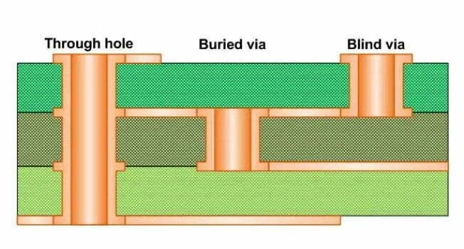
Through-Hole PCBs: Ultimate Resource Guide
Through-hole PCB design: components, soldering, and pros/cons vs SMT. Best practices, tools, and project examples. Essential for beginners and engineers!
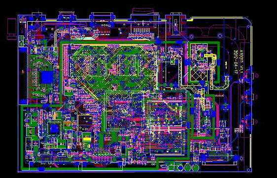
6 Layer PCB Manufacturing Process: The Complete Guide For PCB Designers and Manufacturers
What is 6-Layer PCB Manufacturing? 6-layer PCB manufacturing is the mass-production of PCBs with a minimum of six layers. In a 6-layer PCB, the top and bottom layers are usually

How Much Does PCB Prototyping Cost?
Interactive Guide to PCB Prototype Costs PCB Cost Guide Overview Cost Drivers Strategies Calculator Case Studies FAQ OverviewCost DriversStrategiesCalculatorCase StudiesFAQ Decoding PCB Prototype Costs Welcome to the Interactive Guide to
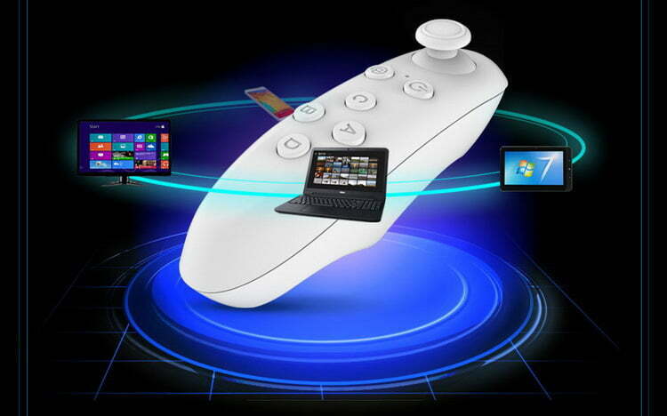
PCB Design of VR Game Controller
VR Gaming Technology Virtual Reality (VR) gaming technology is a rapidly advancing field that enables players to immerse themselves in a computer-generated 3D environment. With advances in hardware and software,
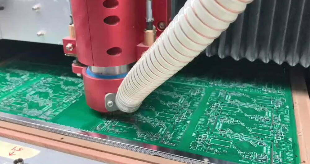
Rapid PCB Prototyping
We have advanced equipment to support rapid PCB prototyping. Depending on the situation, the entire production process takes about one to three weeks. The prototype is first tested in the

PCB Design for Capacitance Test Based on Single Chip Microcomputer
This circuit is based on the PCB design of the capacitance test circuit of the PlCl6LF874 microcontroller. The specific contents are as follows. How the Capacitance Measurement Module WorksThe overall
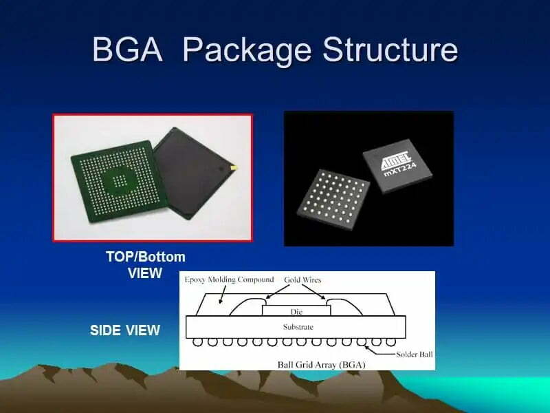
Routing Rules of BGA package in PCB design
BGA is a commonly used component on PCB, usually CPU, NORTH BRIDGE, SOUTH BRIDGE, AGP CHIP, CARD BUS CHIP, etc. They are mostly packaged in bga type. In short, 80%

PCB Design of Temperature Control for LED Home Appliances
1. Develop and design cooperation methods:Software design: MCU software development and design, according to customer requirements, write the required functional software; or rewrite the software part according to the customer’s

