PCB Design Cases

The Ultimate Guide to PCB Vias
Learn via types: through-hole, blind, buried, and vias-in-pad. Tips for spacing, drilling, and reliability in multi-layer PCBs. Essential for advanced layouts. Guide inside!

JFETs: Operation & Circuit Design Guide
Junction Field-Effect Transistors: N-channel/P-channel basics, biasing, and advantages over MOSFETs. Ideal for low-noise amplifiers. Datasheet tips inside!

TRIAC Dimmer Guide: Circuit Design & Use
TRIAC dimmers for AC lighting: operation, phase control, and safety circuits. Learn to design with optocouplers and heat sinks. Project examples inside!

CMOS Technology: History, Manufacturing Process, Application
CMOS, or Complementary Metal Oxide Semiconductor, is a crucial component in various electronic devices, particularly in computers. This article aims to provide a comprehensive understanding of CMOS, its history, functions,
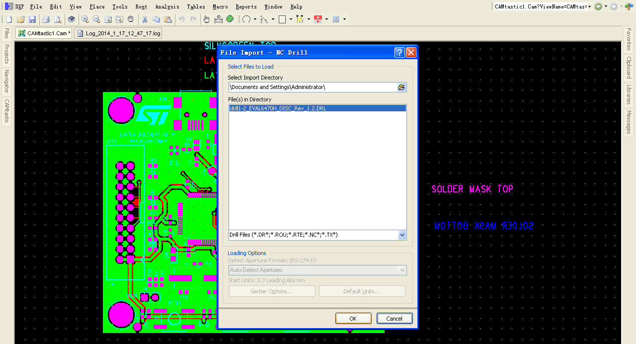
How to Convert Gerber to PCB?
There are many articles on how to convert Gerber to PCB on the Internet, but most of them simply list a few steps. This article aims to introduce the process
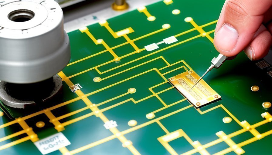
HASL Surface Finish: PCB Design Guide
Hot Air Solder Leveling (HASL) basics: pros/cons, lead-free options, and compatibility. Learn to specify HASL for cost-effective PCBs. Best practices inside!
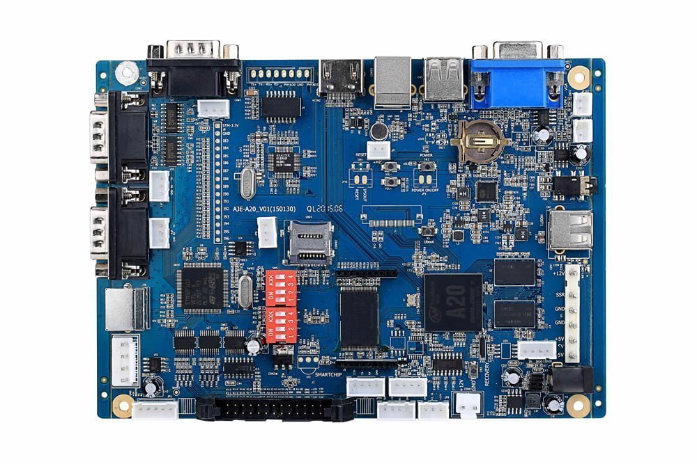
Motherboards Explained: Components & Design Tips
Understand motherboard architecture: CPU sockets, buses, and PCB layers. Tips for selecting components and optimizing layout. Essential for system design. Guide here!
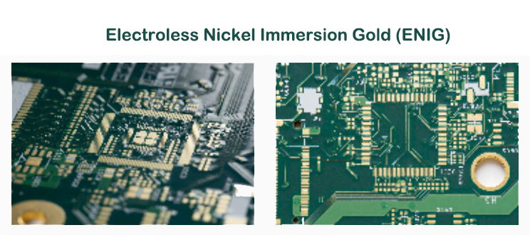
ENIG Surface Finish: PCB Design Guide
ENIG (Electroless Nickel Immersion Gold) basics: thickness, pros/cons, and applications. Learn to specify ENIG for lead-free PCBs. Best practices inside!

