With the continuous deterioration of urban air quality, the air purifier in the car has become a hot-selling product in the automotive supplies. This article introduces our reverse design case of a car air purifier.
Reverse Design of Car Air Purifier
The full process of reverse engineering on the car air purifier including:
- Functions Design;
- Making Circuit Board diagram;
- PCB to Schematics.
We will help you learn from the details of these steps.
Function Design
According to the customer’s requirements, we will implement the following functions for this air purifier:
1. Drive mode - manual and automatic mode
Manual: adjustable resistance (voltage signal); automatic: air quality sensor (voltage signal). The voltage signal is then amplified by the amplifier to control its operation.
2. LED Lights - Automatic recognition of air quality
Design three gear LED indications (buzzer prompts). Then use the comparator to distinguish the three states, and output signals to the three LED lights and the same buzzer.
3. Speed adjustment
Generate a triangular wave by building a hysteresis comparator, use an adjustable resistor (manual) or an air quality sensor (automatic) to cut the triangular wave and then generate a PWM wave through a comparator, and use a push-pull circuit to increase the driving capacity and control the MOS switch to adjust the speed motor.
Making Circuit Board Diagram
How to get the circuit board diagram from an real air purifier? It’s a common steps that is similar to any other products.

Schematic Analysis
According to the target functions and above pcb diagram, we can generate the all schematic diagrams of the air purifier module as follows:
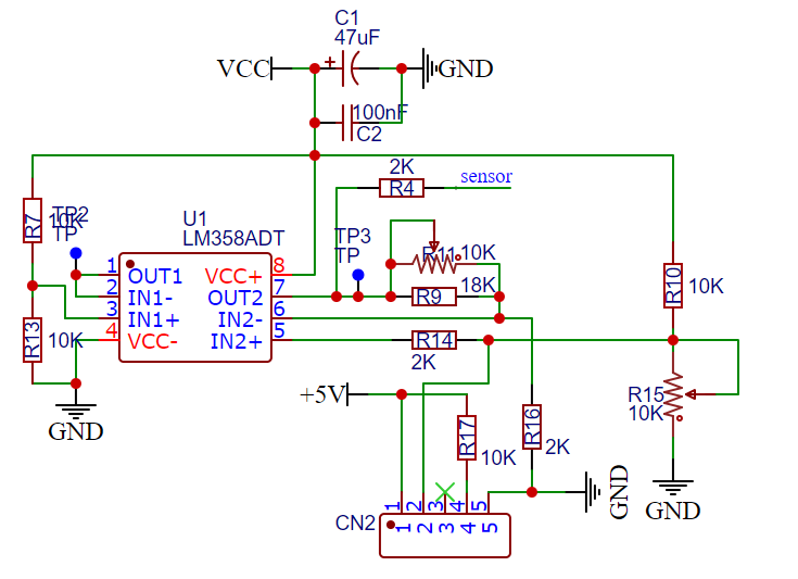
1. air quality sensor
In air quality sensor, a voltage signal is generated by an adjustable resistor or an air quality sensor, and the voltage signal is amplified by an amplifier to drive the motor, LED indication and buzzer sound.
2. LDO (low dropout regulator)
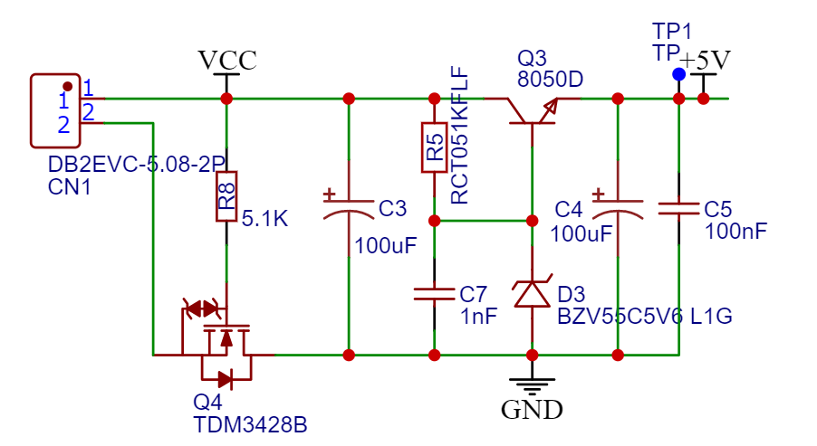
- Q4NMOS tube realizes anti-reverse connection function;
- The NMOS model can be selected according to the specific power consumption of the subsequent circuit;
- R5 is used to limit the current while ensuring the normal operation of D3 (generally above 2mA);
- Q3 normal conduction (1~3mA) amplification;
- C7 is used for filtering;
- The voltage on D3 is stabilized at about 5.6V (the voltage drop is about 0.7V);
- Vce is about 5V, and the current is about 200mA.
3. Air status buzzer
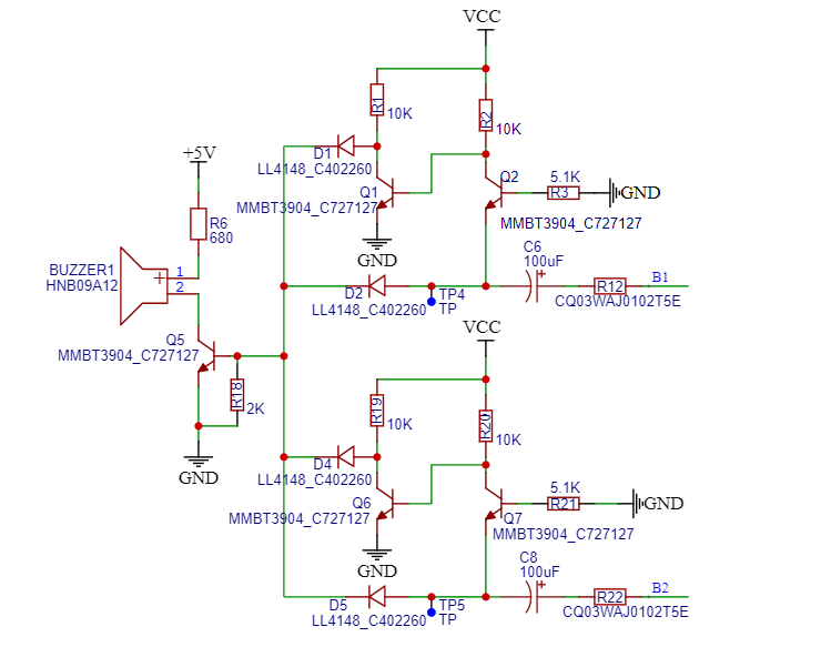
- Ⅰ. When switching from good to medium air quality gear:
B1 is high level (normally low), charges C6 through R13 current limiting, and prevents interference between levels through D2 single-phase continuity. After reaching the Q5 threshold voltage, Q5 is turned on, and the buzzer sounds. The time is determined by R13 and C6 (R*C), until C6 is fully charged (equal to B1 voltage).
- Ⅱ. When switching from medium to poor air quality gear:
B2 is consistent with “Ⅰ”.
- Ⅲ. When the air quality gear is switched from poor to medium:
C8 is discharged through R21, and Q5 is turned on until it is lowered to the threshold voltage, and the sound stops. Ensure that the charging resistance and the discharging resistance are consistent, and the sounding time is basically the same.
- Ⅳ. When switching from medium to good air quality gear:
C6 is consistent with “Ⅲ”.
4. PWM speed Adjustment
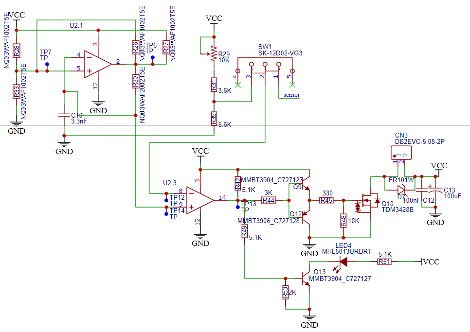
In the schematic of PWM speed:
Two threshold voltages of 5V and 9V are generated by the hysteresis comparator, and C3 is charged in series with R27 and R30. When it reaches the threshold of 9V, it is discharged through R30, and after it is placed at 5V, it is charged to 9V, and then placed at 5V. Cycle Reciprocating, so that a triangular wave oscillating back and forth between 5V and 9V is generated on C3, and the frequency is determined by C3 and R30 (RC);
Then an adjustable DC voltage is generated by an adjustable resistor voltage divider circuit, and a PWM wave with an adjustable duty cycle can be generated by tangent to the triangular wave;
Q9 and Q12 form a push-pull circuit to increase the driving current of the MOS tube;
To reduce the switching loss of the MOS tube, there are two ways: one is to increase the gate voltage (it cannot exceed its limit), and the other is to increase the gate drive current, and at the same time prevent oscillation.

