PCB silkscreen gets treated like decoration right up until somebody tries to assemble, inspect, probe, or repair the board. Then the missing reference designator, buried polarity mark, or unreadable connector label becomes a very real cost. A good silkscreen layer does not make a board pretty. It makes human interaction safer and faster.
That matters most on boards that still depend on technician judgment. Prototype builds, debug spins, mixed-technology assemblies, and field-serviceable products all benefit when the board itself explains what is installed where, which way a part faces, and where a probe should land.
Start with the moments when people must read the board
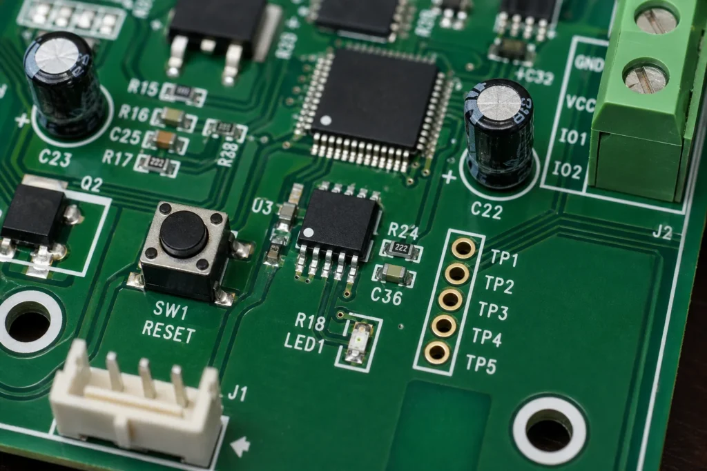
The right way to design PCB silkscreen is to ask who reads it and at what stage. Placement operators may need polarity or pin-1 cues. AOI setup and first-article inspectors may need reference designators that remain visible after assembly. Service technicians may need connector names, test-point labels, or fuse references months later, when the assembly drawing is not open in front of them.
That is why silkscreen decisions belong inside normal PCB layout review, not as a last-minute cosmetic pass. If your team already reviews surface mount PCB layout choices for yield and inspection, silkscreen should be part of that same conversation.
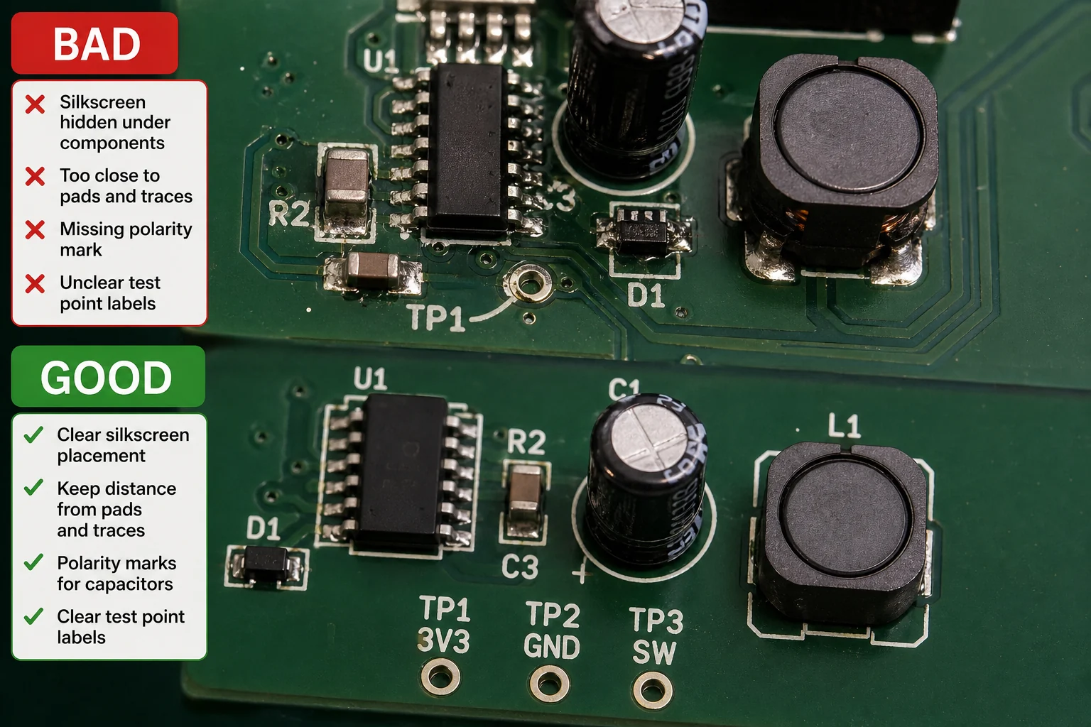
What belongs on silkscreen and what should stay off it
Useful silkscreen usually includes reference designators for key parts, diode and electrolytic polarity, pin-1 orientation, connector identifiers, switch positions, fuse labels, test-point names, board revision, and any assembly note that prevents a likely mistake. The exact mix depends on density and intended service life.
What should stay off the board is equally important. Repeating every small passive reference on a tightly packed side can reduce readability rather than improve it. Long marketing text, oversized logos near working labels, and labels forced into solder-mask slivers often get clipped, smeared, or hidden under components. The result is visual noise instead of guidance.
Common silkscreen mistakes that create downstream trouble
The most common mistake is placing text where the component body will cover it. That sounds obvious, yet it still happens after final placement adjustments. Another frequent problem is printing too close to exposed copper or pad edges, where the fabricator must clip or shift the legend. Once that happens, the surviving text may no longer indicate the right part.
A more subtle mistake is inconsistent orientation. If one connector label reads left-to-right, the next is upside down, and polarity marks move style from part to part, technicians slow down. That does not always show up in design review, but it becomes obvious during rework and debug. Boards that need frequent probing should also avoid tiny test-point labels that disappear under conformal coating or flux residue.
Silkscreen should support rework and service, not only first assembly
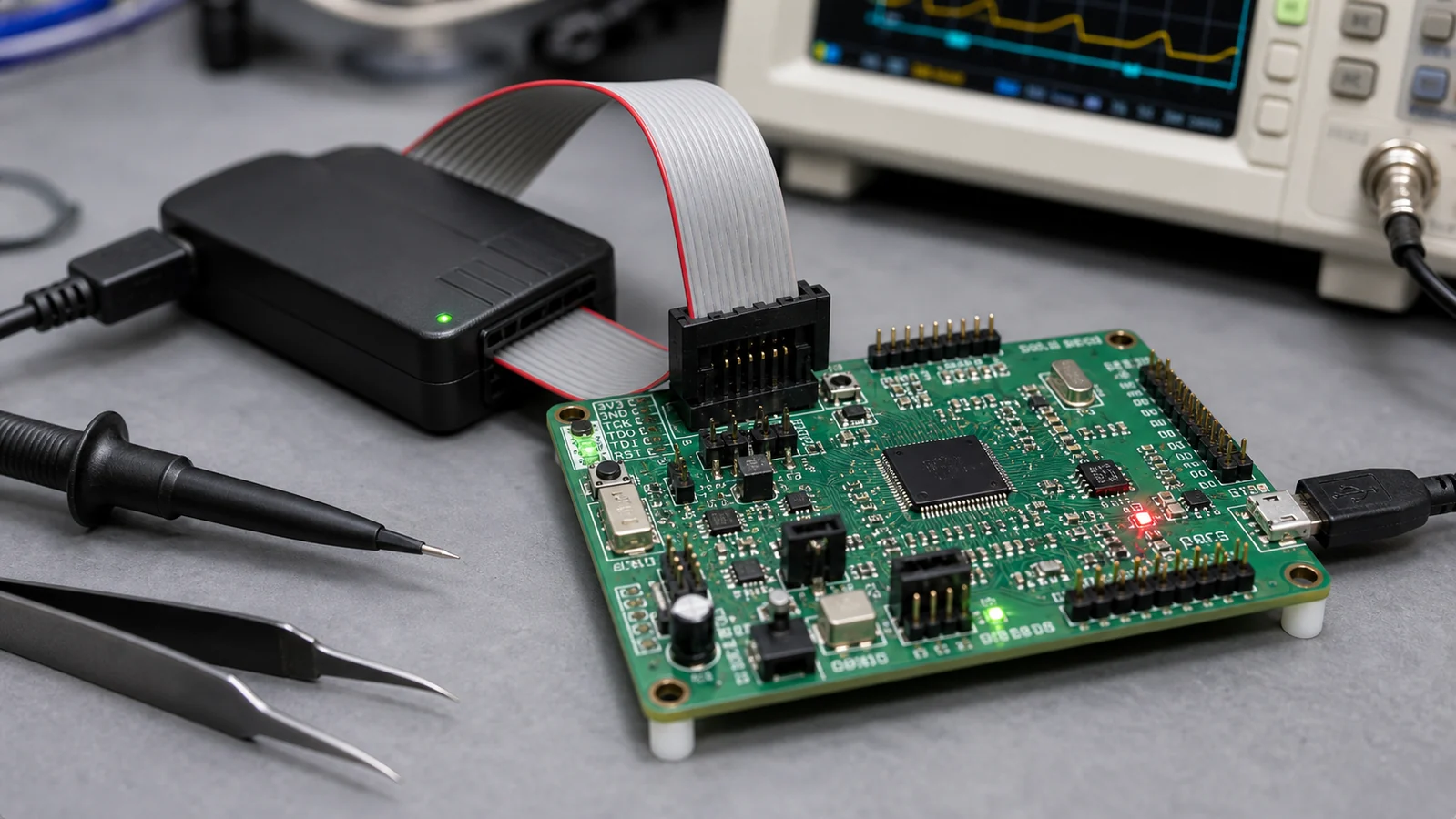
Many boards are easy to assemble once and still annoying to service later. A readable silkscreen layer gives future technicians a map: connector names, board orientation, jumper states, programming headers, fuse references, and polarity cues that survive years after the product leaves the bench. That is especially useful around connectors and debug interfaces such as JTAG connector pinouts and layout checks, where board-side labeling prevents avoidable mistakes.
For dense boards, not every reference has to remain fully visible on the fabricated assembly. But the critical ones should. If a part is likely to be replaced, measured, or orientation-checked, its silkscreen should be treated as a service feature, not as optional artwork.
Use fabrication limits early instead of fixing legend collisions late
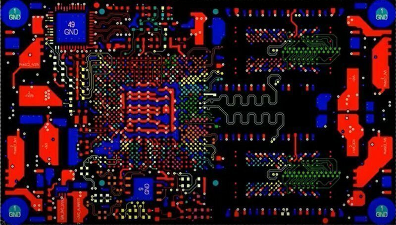
Every fabricator has practical limits on text height, line width, and clearance to pads and mask openings. If those rules are ignored until output generation, the CAD tool or board house will silently clip the legend. Teams using modern electronic design automation tools should turn those rules into repeatable checks so silkscreen violations are caught before final release.
A strong PCB silkscreen layer does a simple job well: it puts the right information in the right place, at a readable size, for the moments when humans need the board to explain itself. That is not decoration. It is risk control for assembly, debug, and field service.
A practical silkscreen review before fabrication release
Before the board files leave layout, zoom in on the areas most likely to cause confusion: connectors, power entry, programming headers, fuses, polarized parts, test points, and any section likely to be reworked. Ask whether the legend is still readable once the component body is present and whether a technician could identify the right point under bench lighting instead of ideal CAD colors.
It is also worth printing a 1:1 paper check for dense boards. Many silkscreen decisions look acceptable on screen and fail once real text size, probe access, and hand placement are considered. That extra review step is cheap compared with assembly hesitation or service mistakes that repeat for the life of the product.
For outsourced assembly, the silkscreen layer also acts as a communication backup when package markings are faint, when alternate components have slightly different body outlines, or when a board returns from debug with handwritten notes that need to be reconciled against the original design intent. Clear board-side labeling shortens that loop.