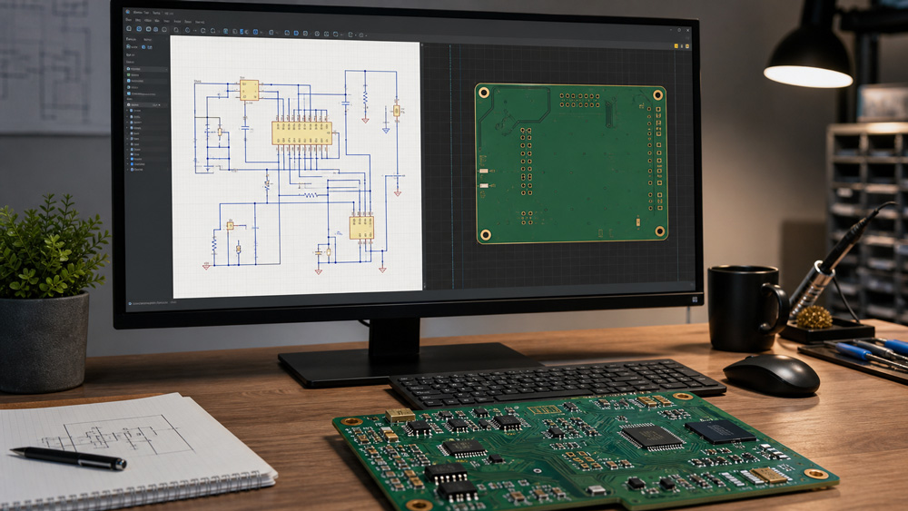
Turning a finished schematic into a PCB layout can feel exciting, but it can also be confusing the first time. Your circuit finally moves from symbols and wires into a real board shape, with parts, copper, layers, and manufacturing limits.
In Altium Designer, learning how to create a new PCB in Altium from a schematic does not mean drawing the PCB again by hand. You create a PCB document, send the schematic data to it, review the Engineering Change Order, and then build the layout into a board that can actually be made. This guide walks through the full workflow, from project setup and footprint checks to component placement, routing, design rules, and common beginner problems.
Before You Start: Check Your Schematic and Project Setup
Before creating a PCB from your schematic, make sure the design is inside a proper Altium PCB project. The schematic file and PCB file should belong to the same project. If the schematic is open as a free document, Altium may not update the PCB the way you expect.
Save the project and compile it before moving on. Compiling helps Altium find problems such as duplicate designators, missing component data, broken net labels, and other issues that can affect the PCB import. Fix serious errors before creating the PCB layout.
Check that every component has a valid PCB footprint. A schematic symbol shows the electrical part, while the footprint defines the real pads and body shape on the board. If a connector, IC, resistor, capacitor, or diode has no footprint, it may fail during the ECO process.
Also check that your parts are annotated. Each component should have a unique designator, such as R1, C3, U2, or J1. Clean designators, assigned footprints, and a compiled project make the schematic-to-PCB transfer much easier.
Step 1: Create or Open Your PCB Project in Altium
Start by opening the PCB project that contains your schematic. In Altium Designer, the project keeps related design files together, including schematic documents, PCB documents, libraries, settings, and output files.
If you already have a project, open it from the Projects panel and confirm that your schematic appears under the project name. If the schematic is listed outside the project, add it before continuing.
If you are starting fresh, create a new PCB project by selecting File > New > Project > PCB Project. Then create or add your schematic document inside that project. Save the project with a clear name, such as Sensor_Board.PrjPcb or Power_Module.PrjPcb.
Keeping the schematic and PCB document in the same project allows Altium to compare them, create ECOs, and keep the design synchronized as you make changes.
Step 2: Add and Save a New PCB Document
After your schematic is part of the project, add a new PCB document. In the Projects panel, right-click the project name and choose Add New to Project > PCB. Altium will create a blank PCB layout file.
You can also create a PCB file from the main menu with File > New > PCB. If you use that method, check that the new PCB document is added to the correct project.
Save the PCB document with a clear file name, such as Main_Board.PcbDoc or USB_Controller.PcbDoc. This file will hold the physical layout for your schematic design.
At this point, the PCB document is still empty. It does not yet contain the schematic components or net connections. Those come in when you update the PCB from the schematic and execute the ECO.
Step 3: Configure the Blank PCB Board
Configuring the blank PCB board means setting the board shape, units, grid, layers, and origin before importing schematic data. This gives you a cleaner workspace before the schematic data arrives.
Start with the board shape. In the PCB editor, use Design > Board Shape to define the outline. You can use a simple rectangle, draw a custom shape, or import a mechanical outline if the PCB must fit inside an enclosure.
Next, set the units and grid. Use millimeters or inches based on your design standard. Pick a grid that makes placement easy, especially for connectors, mounting holes, ICs, and mechanical features.
Review the layer stack as well. A simple microcontroller board may only need two layers. A denser board with high-speed signals, controlled impedance, or cleaner power distribution may need four or more layers.
For a very simple board, compare your stackup plan with single-sided PCB design limits before committing to the layout.
Set the origin in a practical location, such as the lower-left corner of the board. A clear origin helps with placement, measurements, fabrication drawings, and pick-and-place outputs.
Step 4: Import Changes from the Schematic to the PCB
Now transfer the schematic data into the PCB document. With the PCB file open, go to Design > Import Changes From [Project Name]. In some workflows, you can also start from the schematic editor by using Design > Update PCB Document.
Altium will compare the schematic with the PCB layout and prepare a list of changes. This list becomes the Engineering Change Order. It usually includes components, footprints, nets, component classes, and other design data.
Review the ECO before applying it. Check that the components and footprints look correct. If a part has no footprint, or if the footprint library cannot be found, Altium may show an error.
Click Validate Changes first. This checks whether Altium can apply each item in the ECO. If validation passes, click Execute Changes. Altium will then add the schematic components and net information to the PCB document.
After the import, the components may appear outside the board outline or grouped in one area. That is expected. The next job is to review the ECO result and begin component placement.
Step 5: Review and Execute Engineering Change Orders
The Engineering Change Order is the checkpoint between the schematic and the PCB layout. It shows what Altium plans to add, remove, or update in the PCB document.
Read through the ECO before you execute it. Common items include adding components, adding nets, changing footprints, creating classes, and updating component parameters. This review can catch missing footprints, wrong designators, or unexpected net changes early.
Click Validate Changes before executing the ECO. If an item fails, read the message and fix the source problem. The issue may be in the schematic, the library, the project setup, or the footprint mapping.
One common issue is a pin-to-pad mismatch. For example, a schematic symbol may have pins named 1, 2, and 3, while the footprint pads use A, B, and C. In that case, Altium may not know how to connect the symbol pins to the footprint pads.
Once validation succeeds, click Execute Changes. After execution, confirm that each item completed successfully. Then close the ECO window and check that the components and connection lines appear in the PCB editor.
Step 6: Arrange Components on the PCB Layout
After the schematic data is imported, move the components onto the board and create a sensible placement. Good placement makes routing easier and reduces electrical and mechanical problems later.
Place fixed-position parts first. Examples include a USB-C connector on the board edge, mounting holes that match the enclosure, indicator LEDs that must line up with a front panel, or a sensor that needs exposure to air, light, or motion. These parts often define the rest of the layout.
Group related parts together. Keep the fuse, protection diode, regulator, input capacitors, and power connector close together so the high-current path stays short. Keep decoupling capacitors close to IC power pins. Place signal conditioning parts near the sensor or connector they support.
Use the ratsnest connection lines as a guide. Shorter, cleaner connection lines usually mean easier routing. Rotate parts when it helps reduce crossed connections, but keep pin orientation and silkscreen labels readable.
Take your time with placement. It affects board size, routing difficulty, signal quality, heat flow, and assembly. A clean placement can save far more time than rushing into routing.
For broader placement and routing planning, use practical PCB layout guidelines as a checklist while arranging parts.
Step 7: Set Design Rules Before Routing
Before routing traces, set the basic design rules for the PCB. These rules tell Altium what spacing, width, layer, and via choices are allowed.
Start with clearance rules. Clearance is the minimum space between copper features, such as traces, pads, vias, and polygons. Use values that match your PCB manufacturer’s limits.
Set trace width rules next. A 5V input trace feeding several modules may need to be wider than a GPIO signal between a microcontroller and an LED. You can create different rules for power nets, ground nets, and general signal nets.
If trace sizing is still new, review PCB trace basics before setting power and signal widths.
Review via sizes, routing layers, solder mask expansion, and polygon connection settings. For more advanced boards, you may also need impedance rules, differential pair rules, or length-matching rules.
Setting rules before routing helps Altium warn you while you work. It is much easier to fix a trace width or clearance issue during routing than after the whole board is complete.
Step 8: Route the PCB and Check Connectivity
After placement and rule setup, begin routing the PCB. Routing means drawing copper traces that connect pads according to the nets imported from the schematic.
Use the ratsnest to decide the routing order. Start with nets that are harder to fix later, such as the main power path, crystal or clock traces, USB differential pairs, motor current paths, and sensitive analog sensor signals. Then route the simpler signal nets.
Interactive routing in Altium helps you draw traces while following the design rules. If a route violates clearance, width, or layer settings, Altium can warn you. Use vias when a connection needs to move from one layer to another.
After routing, check that all nets are connected. Look for remaining unrouted connection lines. Use the PCB panel and design rule check tools to find open nets, shorts, clearance problems, or routing mistakes.
Do not send the board out just because the traces look finished. Run a design rule check and confirm that the PCB still matches the schematic.
Common Problems When Creating a PCB from a Schematic
Several problems can appear when you create a PCB from a schematic in Altium. Most come from missing footprints, project setup mistakes, or schematic-to-PCB synchronization issues.
Missing footprints are one of the most common problems. A schematic symbol may look correct, but Altium needs a PCB footprint to place the real part on the board. Check the component properties and make sure each part has a valid footprint model.
Components may also fail to appear in the PCB document. This can happen if the schematic is not part of the active PCB project, the wrong PCB document is being updated, or the ECO was not executed.
Net problems can come from unclear net labels, incorrect ports, uncompiled project changes, or symbol pins that do not match footprint pads. Compile the project and review warnings before importing changes.
ECO validation errors often point to the exact source of the problem. For example, a connector may use a schematic symbol named J1, but its selected footprint may point to a library that is not installed on your computer. Other errors may come from duplicate designators, invalid component data, or footprint mismatches.
If the PCB does not match the schematic after edits, update the PCB from the schematic again. The normal Altium workflow is not a one-time transfer. You may repeat the update process many times as the design changes.
Best Practices for Schematic-to-PCB Workflow in Altium
The best schematic-to-PCB workflow in Altium keeps the project organized, footprints verified, and design checks running throughout the layout process. Store the schematic, PCB document, libraries, and output files under the same project structure.
Annotate the schematic before transferring it to the PCB. Each component should have a unique designator, such as R1, C1, U1, or J1. Duplicate designators can create confusing ECO results.
Assign and verify footprints early. Pay special attention to connectors, IC packages, polarized parts, and mechanical parts. A wrong footprint can lead to a board that is difficult or impossible to assemble.
Compile the project before major PCB updates. This helps catch wiring errors, duplicate nets, missing models, and other issues before they reach the layout.
Update the PCB in small steps when possible. After a major schematic change, run the ECO, review the proposed updates, and confirm that the PCB changed as expected.
Run DRC often. Do not wait until the final day to check clearances, unrouted nets, shorts, and rule violations. Early checks make problems easier to fix.
Before manufacturing, also review the board in 3D if your design uses tall connectors, heat sinks, displays, or enclosure constraints. Then generate the needed output files, such as Gerber or ODB++, drill files, BOM, assembly drawings, and pick-and-place data.
FAQ
Can Altium automatically convert a schematic into a finished PCB?
No. Altium can transfer schematic data into a PCB document, including components, footprints, nets, and classes. You still need to place parts, set rules, route traces, check the layout, and prepare manufacturing files.
Do I need a netlist to create a PCB from a schematic in Altium?
Usually, no. In the normal Altium Designer workflow, the schematic and PCB are synchronized directly inside the project. The Engineering Change Order handles the transfer of design data.
Why are my components not showing in the PCB layout?
The schematic may not be part of the active PCB project, the PCB document may not be saved in the project, or the ECO may not have been executed. Missing footprints can also stop parts from being placed correctly.
Why does Altium show missing footprint errors?
A schematic symbol needs a matching PCB footprint. If the component has no footprint assigned, or if the footprint library cannot be found, Altium cannot place that part correctly in the PCB document.
What if my nets import incorrectly?
Check net labels, ports, harnesses, and sheet connections in the schematic. Then compile the project and update the PCB again. Also check whether the footprint pad numbers match the schematic symbol pin numbers.
Can I update the PCB after changing the schematic?
Yes. After editing the schematic, update the PCB again and review the new ECO. Altium will list the differences between the schematic and PCB so you can apply the changes.
What should I check before sending the PCB to manufacturing?
Run a design rule check, confirm all nets are routed, inspect component placement, verify footprints, check board dimensions, review copper pours, and generate the correct manufacturing and assembly files.
Conclusion
To create a new PCB in Altium from a schematic, start with a clean project, assigned footprints, and a saved PCB document. Then use the ECO process to import the design, place parts carefully, set rules, route traces, and run checks. Begin with a small board or test project so each step feels manageable. If the project is beyond practice work, a PCB design service can help turn the schematic into a manufacturable layout. Open your schematic, create the PCB document, and run your first ECO today.