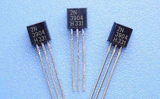
In the mid-1960s, Motorola Semiconductor registered the 2N3906 PNP and 2N3904 NPN transistors in plastic TO-92 packages. Since such transistors are widely available at low cost and robustness, they are available in large numbers to beginners and researchers. In this article, we’ll introduce the 2N3904 transistor specification, its’ working principle, applied circuit example, equivalent transistor, and applications.
2N3904 Transistors Description
2N3904 transistors are a NPN type bipolar junction transistor (BJT) made of silicon material. They are commonly used in electronic circuit applications as a switch or amplifier.
2N3904 Specification
- Current – Collector (Ic) (Max): 200mA
- DC current gain or hFE (Max): 300
- DC current gain or hFE (Min): 100 @ 150mA, 10V
- Collector to emitter voltage (Vce) : 40V
- Base to emitter voltage (Vbe): 6V
- Collector to base voltage (Vcb): 60V
- Vce saturation (maximum) under Ib, Ic conditions: 500mV @ 50mA, 500mA
- Power – Max: 800mW
- Frequency – Conversion: 100MHz
- Package/Case: TO-39-3, TO-205AD
2N3904 Pinout Configuration

The 2N3904 Transistor consists of three pins:
- Pin1 (Emitter): Current will flow through this terminal.
- Pin2 (Base): This pin controls the transistor bias.
- Pin3 (Collector): Current supply for the entire terminal.
2N3904 Datasheet & Semiconductor Structural Parameters
When designing high-reliability circuits or performing PCB reverse engineering, understanding the official 3904 transistor datasheet metrics is critical for hardware clones and circuit replication. The 2n3904 data sheet defines this device as a classic npn 2n3904 silicon bjt 2n3904 tailored for general-purpose low-power applications.
Looking deeper into the physical layout of this 2n transistor, the 2n3904 transistor doping levels emitter base and collector are engineered with precise profiles: the emitter region features heavy n-type doping to maximize carrier injection, while the base region is ultra-thin and lightly p-doped to minimize recombination. This structural configuration determines the critical electrical boundaries of the 3904 transistor, such as the 2n3904 max current rating restricted to 200 mA continuous collector current (IC). For comprehensive circuit layout validations, downloading a verified npn 3904 datasheet ensures your thermal and biasing tolerances remain well within safe operating limits.
2n3904 Transistors Working Principle
In a 2N3904 transistor, most of the charge carriers are electrons, so they are always negatively charged. The state of this transistor can change from reverse biased to forward biased to conduct depending on a small voltage at the base terminal ( such as 0.7V).

Normal operating conditions:
- Base voltage (Vb) > emitter voltage (Ve).
- Collector voltage (Vc) > Base voltage (Vb).
If the base pin is connected to the GND terminal, both the emitter and collector terminals are reverse biased or left open. Similarly, once a signal is given to the base pin, it will be forward biased.
The high gain value of the 2N3904 transistor is 300, which determines its amplification ability. The maximum current supply across the collector terminal is 200mA, so loads consuming more than 200mA cannot be connected via this transistor. Once the current supply is given to the base terminal, the transistor can be biased. This IB current must be limited to 5mA.
When the 2N3904 NPN transistor is completely biased, it permits a maximum of 200mA to flow through two specific terminals, namely emitter and collector. This particular stage is referred to as the saturation region. Moreover, the collector-emitter/collector-base terminals are capable of handling typical voltages of 40V and 60V respectively.
Once the base current separates, the transistor will turn off, so this phase is called the cutoff region, and the VBE may be around 600mV.
2n3904 Circuit Example
The LED flash circuit using 2N3904 transistor is shown in the figure below. The circuit can be built using basic components like a breadboard, hookup wires, 9V battery, capacitor, 5mm LED, LED flash, 1K, 10K and 4.7K resistors.

This circuit uses a 6V DC battery to power the circuit. Since there is an NPN transistor in this circuit, once the base pin of this transistor is connected to GND, the terminals like emitter and collector are reverse biased. Also, once a signal is supplied to the base pin of this transistor, then it is connected to be forward biased. This simple LED blinking circuit is used in different devices such as doorbells, alarm systems or strobe lights.
2N3904 Vs. 2N2222A Transistors
Here is a comparison of 2N3904 and 2N2222A transistors below:
| Specification | 2N3904 | 2N2222A |
|---|---|---|
| Transistors Type | NPN | NPN |
| Maximum Collector Current | 200 mA | 800 mA |
| Maximum Collector-Emitter Voltage | 40V | 40V |
| Maximum Collector-Base Voltage | 50V | 50V |
| Maximum Emitter-Base Voltage | 5V | 6V |
| Maximum Frequency | 300 MHz | 500 MHz |
| Package Type | TO-92 | TO-18, TO-92 |
2n3904 Equivalent Transistors
Some equivalent transistors to the 2N3904 are:
BC636, BC547, BC549, BC639, 2N2222 TO-18, 2N2222 TO-92, 2N2369, 2N3906, 2N3055, 2SC5200, etc.
2N3904 Application
- Amplifiers
- Drivers modules (LED, Motor, or relay drivers)
- Switches
- Voltage Regulators
- Converters
- Timers
- Frequency Modulators
- PWM (Pulse Width Modulation)
- Signal Processing Circuits
- Audio Circuits
- Power Supply Circuits
- Comparators
2N3904 Transistor Characteristic Frequency Testing
Understanding 2N3904 Max Frequency and Transition Frequency (fT)
Before conducting hardware laboratory verification, it is vital to check the component specifications regarding speed limits. The 2n3904 max frequency—formally logged as the 2n3904 transition frequency ft—is specified as 300 MHz under standard test conditions (IC = 10 mA, VCE = 20 V, f = 100 MHz). This 2n3904 transition frequency ft typical performance allows the n3904 transistor to excel not just in baseband DC switching, but also in high-speed pulse applications and VHF radio-frequency (RF) amplification circuits.
Required equipment:
- Tektronix MSO34-BW500 oscilloscope
- Tektronix AFG31251 signal generator
- Digital multimeter
- Digital source meters *2
- Transistor DC/AC parameter comprehensive experimental board
The characteristic frequency of 2N3904 transistor can be measured by using Tektronix oscilloscopes, signal generators, and Keithley source meter products for AC parameter testing of transistor devices. As the actual operating frequency of the transistor is much higher than the low-frequency current gain cutoff frequency fβ, the AC current gain is inversely proportional to the operating frequency, and the “gain-bandwidth product” of the transistor is constant, approximately equal to the working frequency when the modulus of the common-emitter current gain is 1.
The measurement of the characteristic frequency of bipolar transistors is to couple a high-frequency small AC input signal of a specific frequency to the base through a capacitor, change the DC bias conditions of the common-emitter configuration transistor, and thereby change the AC current gain to study the relationship between the characteristic frequency of the transistor and the DC operating point.
Setting and Testing the Static Operating Point
The working range of the 2N3904 is shown in the following figure:

Deciphering the 2N3904 Characteristic Curves and Vbe Thresholds
The operational boundaries displayed in the 2n3904 characteristic curves plot illustrate three distinct functional zones: the saturation, active, and cutoff regions. In practical switching designs, the 2n3904 vbe (base-emitter voltage) is the gating factor; it typically requires around 0.65V to 0.7V of forward bias for active region conduction, whereas under full saturation conditions, the VBE(sat) can rise up to 0.95V. Engineers utilizing the npn 3904 for small-signal amplification must strictly bias the device along the linear portion of these 2n3904 characteristic curves to avoid clipping and signal distortion, while keeping an eye on the dynamic hfe 2n3904 variations relative to ambient temperature.
To ensure that the transistor operates in the amplification region, the DC operating point of the transistor is set to IC=1mA. When no AC signal is connected, the static working circuit diagram of the transistor is shown in the following figure:

Adjust the IB output of SMU1 and observe that the IC current value of SMU2 is approximately 1mA to ensure that the transistor operates in the amplification region. The IB is approximately 2.8uA, and the BE voltage VBE is 0.636V as measured by a multimeter.
Testing the H-parameters of the 2N3904 Transistor: HIE and HFE
With a reasonable setting of the static operating point and an AC small signal input, the transistor can be equivalent to a linear two-port circuit, represented by AC components of current and voltage. Where Ib and Vbe are the input variables of the transistor, and Ic and Vce are the output variables. The h-parameters of the transistor reflect the small-signal AC characteristics of the transistor under certain fixed static conditions.
Connect the signal generator output to the BNC interface on the left side of the experimental board’s AC IN, and connect the oscilloscope Channel 1 to the BNC interface on the right side of the experimental board’s AC OUT.
Set the signal source output to a 1 kHz sine wave, adjust the signal source output signal amplitude, and use oscilloscope channel 2 to test the voltage waveform between the two terminals of R1 (connect the banana head interface marked as Input). Calculate the effective value of Ib current so that Ib is approximately equal to 0.5 uA.
Set the signal source output to a 1 kHz sine wave and change the output amplitude. When the effective value of the voltage between the two terminals of R1 measured by the oscilloscope is 50 mVrms, and since R1 = 100 kohms, Ib is approximately equal to 0.5 uA.
HIE
“hie” is the input resistance when the output is short-circuited and reflects the ability of the base voltage to control the base current with output voltage Vce unchanged.
ℎ𝑖𝑒 = 𝑣𝑏𝑒/𝑖𝑏 = 𝑣𝑏𝑒/𝑣𝑖𝑛𝑝𝑢𝑡∗ 𝑅1
Under the condition that the above test conditions remain unchanged, the effective value of Vbe measured by 2 channels of the oscilloscope is 5.7mVrms.
hie = Vbe/ib = Vbe/Vib * R1 = 5.7/50 * 100K = 11400, where Vbe is the effective value of the Vbe and Vib is the effective value of the input voltage under the above test conditions.
HFE
HFE is a term commonly used to refer to the “DC current gain” of a bipolar junction transistor (BJT). It reflects the ability of the base current ib to control the collector current ic. Below is the formula of HFE:
ℎ𝑓𝑒 = 𝑖𝑐/𝑖𝑏
𝑖𝑐= voutput / R2
where “𝑖𝑐” stand for the collector current, and “𝑖𝑏” stand for the base current, “voutput” is the effective value of the output voltage, and “R2” is the resistance of the load connected between the collector and the power supply.
Result:
𝑖𝑐= voutput / R2 = 17.3 mV / 100 ohms = 0.173 mA
When performing frequency testing, the quality of the component significantly affects the accuracy of your results. Many engineers rely on specialized PCB Component Sourcing Services to manage their bill of materials (BOM) and ensure every active device meets the specified datasheets.
Calculating Characteristic Frequency (fT)
Measure the transistor’s cut-off frequency fβ and calculate its characteristic frequency fT using the “gain-bandwidth product” method.
Gradually increase the output frequency of the signal source from 1 kHz, and observe the amplitude of the AC OUT signal on the right side of the experimental board using the oscilloscope. When the output signal amplitude drops by 3 dB (peak-to-peak value drops by half), record the output frequency fβ of the signal source, indicating the cut-off frequency of the transistor at the current working point.
At 1 kHz, the AC OUT output peak-to-peak value is approximately 38 mV, and at 1.4 MHz, the AC OUT output peak-to-peak value is approximately 19.2 mV.
Calculate the characteristic frequency fT of the transistor using the gain-bandwidth product formula:
fT = hfe × fβ
fT = 228 * 1.4 = 319.2 MHz
where fβ is approximately equal to 1.4 MHz.
Verify the characteristic frequency fT of the transistor using a high-frequency signal source and a 500 MHz bandwidth oscilloscope. If the bandwidth of the oscilloscope and signal source is greater than 200 MHz, you can use the signal source to scan the input signal in the frequency range above DC-200MHz, and test the amplitude-frequency characteristics of the output signal (AC OUT) on the oscilloscope, and calculate the current magnification down to 1 manually find the characteristic frequency point fT. Verify that the eigenfrequency values calculated by the gain-bandwidth product method are accurate.
Engineering checks for 2N3904 transistor pinout and testing
Before using 2N3904 transistor pinout and testing in a PCB, firmware, repair, or validation workflow, confirm the details that usually decide whether the design works reliably instead of only reading the headline specification.
Design and troubleshooting checklist
| Area | What to check | Why it matters |
|---|---|---|
| Package orientation | Confirm emitter, base, and collector order for TO-92 and SOT-23 variants before matching the footprint | Different manufacturer packages can swap the visible pin order on assembly drawings |
| Switching design | Calculate base current, load current, saturation voltage, and MCU GPIO drive limit | A 2N3904 used as a low-side switch needs enough base drive without overstressing the controller |
| Bench test | Measure diode junctions, leakage, gain range, and heating under the real load current | Simple multimeter tests catch damaged or counterfeit transistors before board rework |
These checks help connect the search intent around 2N3904 pinout with practical board-level decisions, component selection, and failure analysis.
Frequently Asked Questions (FAQ) About the 2N3904 Transistor
1. What is the most reliable 2N3904 equivalent transistor for substitution?
If you cannot source the original 2n 3904, the most direct 2n3904 equivalent options are the 2N2222A or BC547. When selecting a 3904 transistor equivalent, always verify that the package matches; for example, European layouts like the BC547 may have an altered pin sequence compared to the standard TO-92 2n3904 equivalent transistor. In international documentation, you might also look up the 2n3904 equivalente specifications to ensure full cross-compatibility in multi-layered PCB assemblies.
2. Where can I find a standard 2N3904 schematic symbol for EDA software?
A standard 2n3904 schematic layout contains the standard 3-terminal NPN symbol with the emitter arrow pointing outwards. Most ECAD toolsets index this under general-purpose 3904 transistor libraries, allowing you to seamlessly pair it with its PNP complementary counterpart during push-pull amplifier engineering.
3. How does the 2N3904 pinout compare to the 2N4125 pinout?
While both devices are traditionally housed in the classic plastic TO-92 package, they have opposite polarities. The 2N3904 is an NPN device, whereas the 2N4125 is a PNP general-purpose device. Interestingly, when looking at the flat face, the 2n4125 pinout follows the exact same Emitter-Base-Collector (E-B-C) pin configuration sequence as the 2N3904, making them highly intuitive to layout symmetrically on a dual-rail analog PCB.
2N3904 Datasheet Quick Reference
A datasheet 2N3904 lookup usually focuses on pinout, maximum collector current, voltage ratings, gain range, package orientation, and whether the device can replace another small-signal NPN transistor. Always confirm the manufacturer datasheet because limits and test conditions can vary slightly by vendor.
| Parameter | Typical design meaning | Why it matters |
|---|---|---|
| VCEO | Maximum collector-emitter voltage | Sets the safe voltage range for switching |
| IC max | Maximum collector current | Prevents overheating or device failure |
| hFE | DC current gain range | Affects base resistor and bias design |
| VBE | Base-emitter forward voltage | Important for bias and switching threshold |
| fT | Transition frequency | Indicates high-frequency small-signal behavior |
Maximum Collector Current, Power Dissipation, and VBE
The 2N3904 is a small-signal transistor, not a power transistor. Even if the datasheet lists a maximum current, practical designs should include power dissipation, duty cycle, ambient temperature, and package thermal limits before using it as a load switch.
2N3904 Equivalent Transistors and Pin Compatibility
Common 2N3904 equivalent choices may include 2N2222, BC547, S8050, or other NPN small-signal transistors, but they are not always drop-in replacements. Check collector current rating, voltage rating, gain range, package type, and especially the E-B-C pin order before replacing a part on a PCB.