What is PCB Crosstalk?
PCB crosstalk is a voltage noise phenomenon caused by inductive coupling or capacitive coupling between two signal lines.
Types of Crosstalk
According to different sources, there are three different types of crosstalk on the PCB: inductive coupling, capacitive coupling and common resistance coupling.
inductive coupling
Inductive coupling is a process of transferring energy between two objects through an inductive loop. It is a type of electromagnetic coupling, where one wire loop induces an electric current in another wire loop. This type of coupling is commonly used in electrical transformers, where the primary and secondary windings are inductively coupled.
capacitive coupling
Capacitive coupling is the transfer of energy between two electrical conductors through an intervening electrical field. This type of coupling is used in many electronic circuits, such as sensors, filters, and oscillators. It is also used to couple signals from one circuit to another.
common-impedance coupling
common-impedance coupling is a type of electrical circuit connection in which two circuits are connected together by a single resistor. This type of connection reduces the amount of noise in a circuit by ensuring that the signals in both circuits remain at the same level and do not interfere with each other.
How Crosstalk Occurs?
The crosstalk may be caused by the PCB board layer parameters, the signal line spacing, the electrical characteristics of the driving and receiving ends, and the wire termination method.
Inductive and capacitive coupling
In digital circuits, inductive coupling is more common than capacitive coupling due to the low impedance nature of digital drivers. Capacitive coupling is more common in high impedance (usually analog) circuits.
Assume two microstrip lines with a center-to-center distance d, as shown in the figure below.
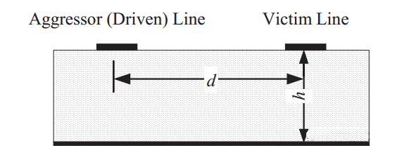
As the signal propagates along the transmission line, electric and magnetic field lines begin to appear around the microstrip line.
However, these electric and magnetic field lines are not just in the signal and its associated loop, but extend into the surrounding area. As shown below.
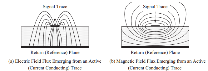
The electric field emanating from the transmission line terminates with any adjacent metallic structures; the magnetic field around the transmission line also partially surrounds any adjacent metallic structures.
What if the adjacent metal structure happens to be a signal transmission line?
Then the transmission line will generate corresponding current and voltage due to the received electromagnetic field generated by the disturbing microstrip line.
Obviously, if the separation between two transmission lines is increased, the field received by the signal transmission line will drop rapidly.
However, if they are close enough, adjacent signal transmission lines will pick up the resulting interference currents. And these interference currents, like the original signal currents on the transmission line, will also experience reflection, distortion and radiation.
crosstalk model
Capacitive coupling and inductive coupling, and their respective effects on crosstalk are largely dependent on circuit layout. As shown in the figure below, it is a simplified model of crosstalk, including capacitive and inductive coupling between transmission lines on the PCB.
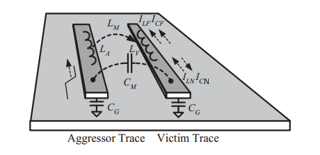
CG, which exists between the microstrip line and the reference plane, affects the characteristic impedance and signal propagation delay of the microstrip line.
CM, existing between microstrip lines, is capacitive coupling.
LA and LV represent the self-inductance of the perturbing and disturbed microstrip lines, respectively, which will affect the characteristic impedance and signal propagation delay of the microstrip line.
LM, which stands for the mutual inductance LM between the two microstrip lines, causes inductive coupling between the two circuits.
Calculation of coupling inductance
In electrically small microstrip lines, capacitive coupling appears as a current source in parallel with the victim line, and inductive coupling appears as a voltage source in series with the victim line. The specific relationship is shown in the following formula:
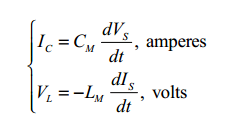
where IC and VL are the capacitively induced current and inductively induced voltage in the disturbed microstrip line, respectively, which are caused by changes in the source voltage VS and current IS in the disturber microstrip line.
reverse crosstalk and forward crosstalk
Capacitive coupling, the capacitive induction current generated on the disturbed microstrip line will propagate to both ends, that is, propagate forward, towards the far-end ICF, and propagate backward, towards the near-end ICN.
Inductive coupling, the inductively induced voltage generated on the disturbed microstrip line, generates a current (ILF, ILN) on the disturbed microstrip line, and its direction is opposite to IS.
Therefore, when the capacitive coupling and inductive coupling signals propagate backward, the currents are superimposed and the coupling is enhanced; when they propagate forward, the current tends to cancel.
The total coupled signal flowing backwards is called “reverse crosstalk” or “near end crosstalk” (NEXT), while the total coupled signal flowing forward (actually canceling) is called “forward crosstalk” or “far end crosstalk” “(FEXT).
common-impedance coupling
The third type of crosstalk in PCB traces is common impedance coupling. It occurs usually when two conductors go through the same return trace. For example, a digital circuit and an analog circuit will leads the common impedance coupling, if they are connected in same end.
Reflow Model for High-Frequency Signals
Most of the return flow of high-frequency signals exists on the reference plane below the microstrip line, but a small part will spread to both sides. Its reflow density on the reference plane can be expressed by the following formula:
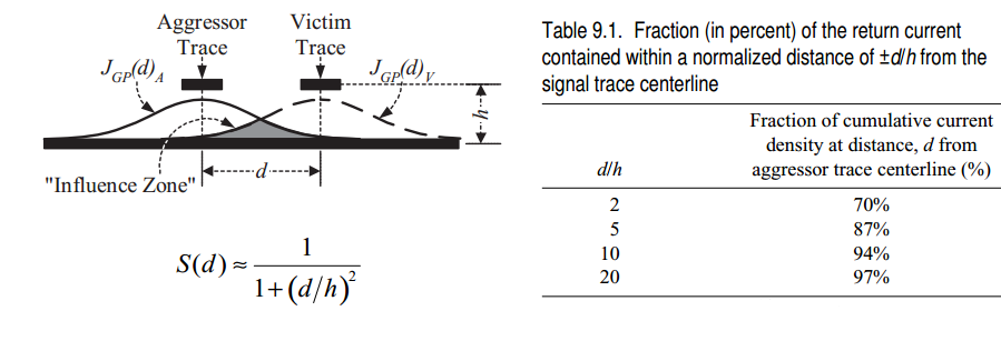
As shown in the figure above, JGP(d)A and JGP(d)V are the current density distributions of the disturbing microstrip line and the disturbed microstrip line, respectively. The part where the two overlap, that is, the gray part in the above figure, is the “influence area”, which determines the degree of influence between the two microstrip lines.


