About PIC18F26K40 Microcontroller
The PIC18F26K40 microcontroller is a powerful and versatile device with a range of advanced features such as strong security, multiple communication interfaces, and energy-saving capabilities. It is designed to meet the demands of high-performance applications while operating with low power consumption, making it a reliable choice for a wide range of electronic designs.
Features
- Designed for high-performance applications
- Wide operating voltage range: 1.8V to 5.5V
- 64KB flash memory and 3.8KB SRAM
- Communication interfaces: SPI, I2C, UART
- 12-bit ADC module with up to 38 channels
- High-speed comparators module with up to 8 channels
- Various peripherals: PWM, ECCP, CLC
- Flexible clocking system with PLL and 31 kHz low-power oscillator
- Advanced security features: hardware crypto engine for AES, DES, 3DES encryption/decryption, and memory protection
- Low-power features: sleep mode, doze mode
- Suitable for high-performance applications with power-constrained requirements
Parameters
- CPU: 8-bit
- Maximum Clock Frequency: 64 MHz
- Program Memory Size: 64KB
- Data Memory Size: 3.8KB
- Operating Voltage Range: 1.8V to 5.5V
- Temperature Range: -40°C to +125°C
- Number of Pins: 28
- Number of Analog Inputs: Up to 38
- Number of Comparators: Up to 8
- Communication Interfaces: SPI, I2C, UART
- Peripherals: PWM, ECCP, CLC
- Interrupt Sources: Up to 24
- Timer Modules: Up to 4
- Watchdog Timer: Yes
- Brown-out Reset: Yes
- Low Voltage Detection: Yes
- In-Circuit Debugger: Yes
- Hardware Crypto Engine: AES, DES, 3DES encryption/decryption
- Memory Protection: Yes
- Power-Saving Modes: Sleep mode, Doze mode
- Package Type: Various options, including TQFP, SOIC, and SSOP.
Pinout Configuration

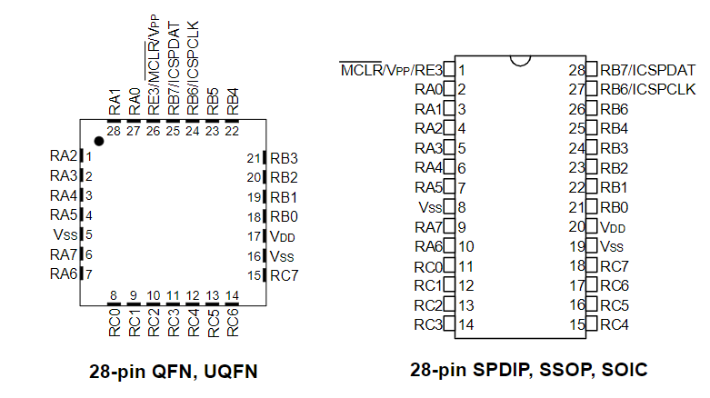
The PIC18F26K40 microcontroller has a 28-pin package that follows a standard pinout configuration. The pins are arranged in two rows with 14 pins in each row, and the spacing between the pins is 0.1 inches. The microcontroller features a range of I/O pins, including general-purpose pins for input and output, analog inputs, and communication interfaces such as SPI, I2C, and UART. In addition to the I/O pins, the microcontroller also has dedicated pins for peripherals such as PWM and ECCP modules. The pinout design of the PIC18F26K40 provides flexibility and versatility for a variety of applications while adhering to a standard configuration for ease of use.
Block Diagram

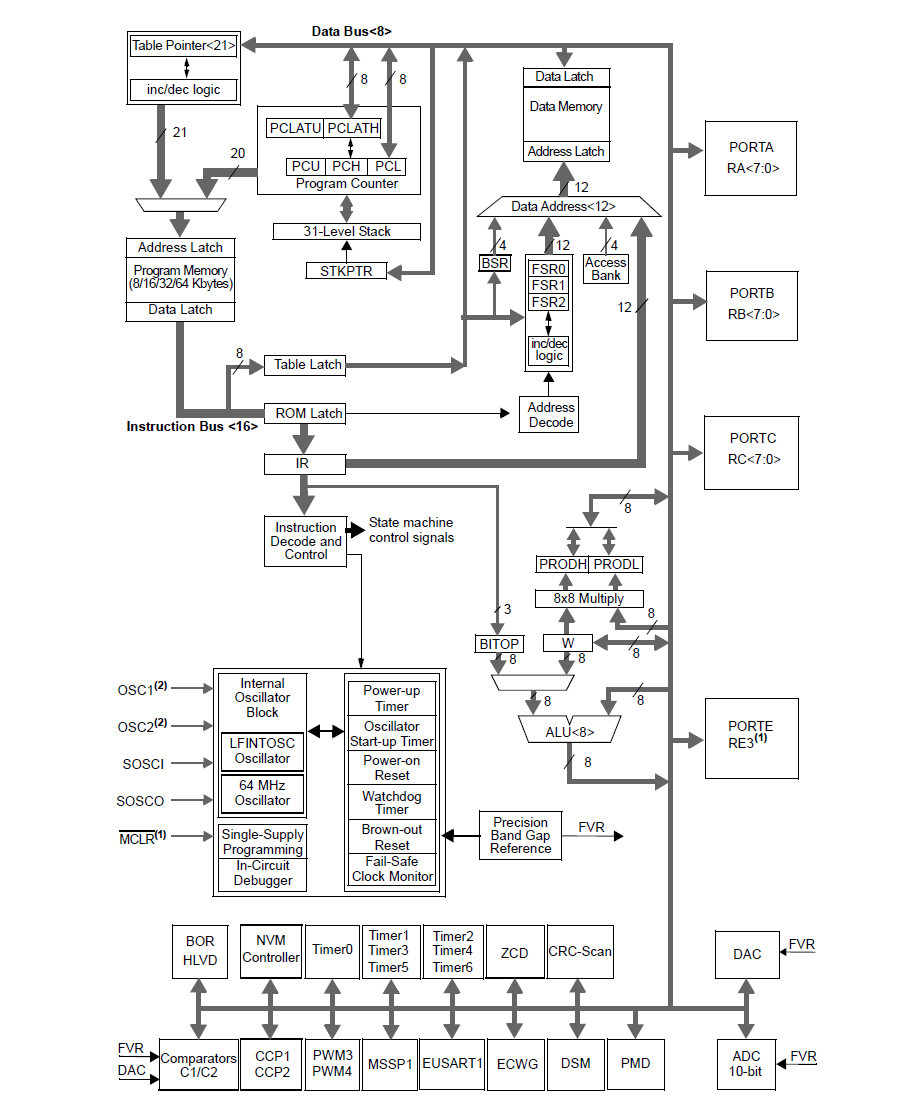
The block diagram of the PIC18F26K40 microcontroller shows the key functional blocks that make up the device. These include a powerful CPU, a range of peripheral modules for communication and timing, a comprehensive memory system, a flexible clocking system, and advanced security features. These functional blocks enable the microcontroller to execute complex tasks and handle a wide range of input/output operations with accuracy and efficiency.
Programming of PIC18F26K40 microcontroller
There’re a variety of programming tools and languages for programming PIC18F26K40, including the MPLAB X Integrated Development Environment (IDE), the XC8 C Compiler, and Assembly Language. The microcontroller can be programmed using in-circuit programming (ICSP) or in-system programming (ISP) techniques.
To start, users first need to create a project in the MPLAB X IDE and configure the settings for the microcontroller, including clock settings, memory mapping, and peripheral configuration. They can then write and compile their code using the XC8 C Compiler or Assembly Language and upload it to the microcontroller using a programming tool such as the PICkit 4 or ICD 4.
let’s consider a simple project that involves turning an LED on and off using a push button. Here are the steps to implement this project:
Hardware setup
Connect a push button to a GPIO pin of the microcontroller and connect an LED to another GPIO pin.
Create a New Project
Create a new project in MPLAB X IDE and select the PIC18F26K40 microcontroller as the target device. Configure the project settings, including clock frequency, memory mapping, and peripheral configuration.
Write the LED Code
Write the code to initialize the GPIO pins for the push button and LED, and define the logic for turning the LED on and off based on the state of the push button. Here’s an example code snippet in XC8 C:
					#define BUTTON_PIN RB0
#define LED_PIN RB1

void main(void)
{
    TRISBbits.TRISB0 = 1; // Set RB0 as input
    TRISBbits.TRISB1 = 0; // Set RB1 as output

    while(1)
    {
        if(BUTTON_PIN == 0) // Check if button is pressed
        {
            LED_PIN = 1; // Turn LED on
        }
        else
        {
            LED_PIN = 0; // Turn LED off
        }
    }
}
Compile the Code
Compile the code using the XC8 C Compiler and upload it to the microcontroller using a programming tool such as the PICkit 4 or ICD 4.
Test the Project
Test the project by pressing the push button and verifying that the LED turns on and off accordingly.
Supported Decryption Models
For some reason you need to unlock your MCU, that’s what we can help with you. Below are our available PIC18 series model:
- PIC18F26K40-E/ML
- PIC18F26K40-E/MV
- PIC18LF26K40-E/ML
- PIC18LF26K40-E/MV
- PIC18F26K40-E/SO
- PIC18F26K40-E/SP
- PIC18F26K40-E/SS
- PIC18LF26K40-E/SO
- PIC18LF26K40-E/SP
- PIC18LF26K40-E/SS
- PIC18F26K40-I/ML
- PIC18F26K40-I/MV
- PIC18F26K40-I/SO
- PIC18F26K40-I/SP
- PIC18F26K40-I/SS
- PIC18LF26K40-I/ML
- PIC18LF26K40-I/MV
- PIC18LF26K40-I/SO
- PIC18LF26K40-I/SP
- PIC18LF26K40-I/SS

Principal Engineer:
Dr. Billy Zheng
Well Done PCB Technology
billy@reversepcb.com
Emergency Support: +86-157-9847-6858


